Semiconductor device and manufacturing method thereof

a semiconductor and semiconductor technology, applied in the direction of semiconductor devices, basic electric elements, electrical equipment, etc., can solve the problems of deteriorating transistor characteristics, adversely affecting the electric characteristics of transistors, boron leakage, etc., and achieve the effect of suppressing boron leakage and increasing the density of the interface sta

Inactive Publication Date: 2008-12-04
ELPIDA MEMORY INC
View PDF7 Cites 20 Cited by
  • Summary
  • Abstract
  • Description
  • Claims
  • Application Information

AI Technical Summary

Benefits of technology

[0009]The present invention has been achieved to solve the above problems, and an object of the present invention is to provide a semiconductor device that suppresses boron leakage

Problems solved by technology

If a thermal load is applied to the dual gate CMOS transistor during steps after the gate electrodes are formed, boron in the gate electrode of the PMOS transistor can pass through a gate insulating film made of a silicon oxide film to diffuse in a silicon substrate (n-well), resulting in a phenomenon that adversely affects electric characteristics of the transistor (boron leakage).
That can lead to deteriorated transistor c

Method used


Image

  • Semiconductor device and manufacturing method thereof
  • Semiconductor device and manufacturing method thereof
  • Semiconductor device and manufacturing method thereof

Examples


Embodiment Construction

[0025]Preferred embodiments of the present invention will be explained below in detail with reference to the accompanying drawings.

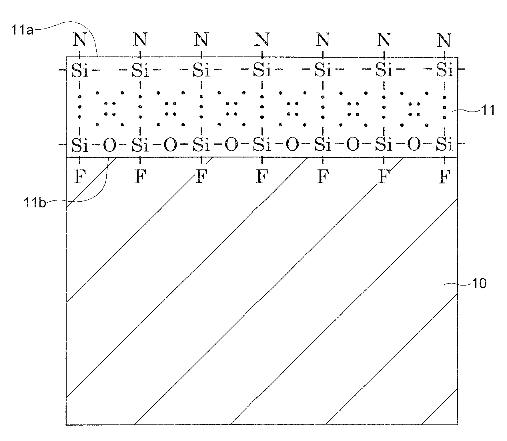
[0026]FIG. 1 is a partial cross-sectional view of configuration of a semiconductor device according to an embodiment of the present invention.

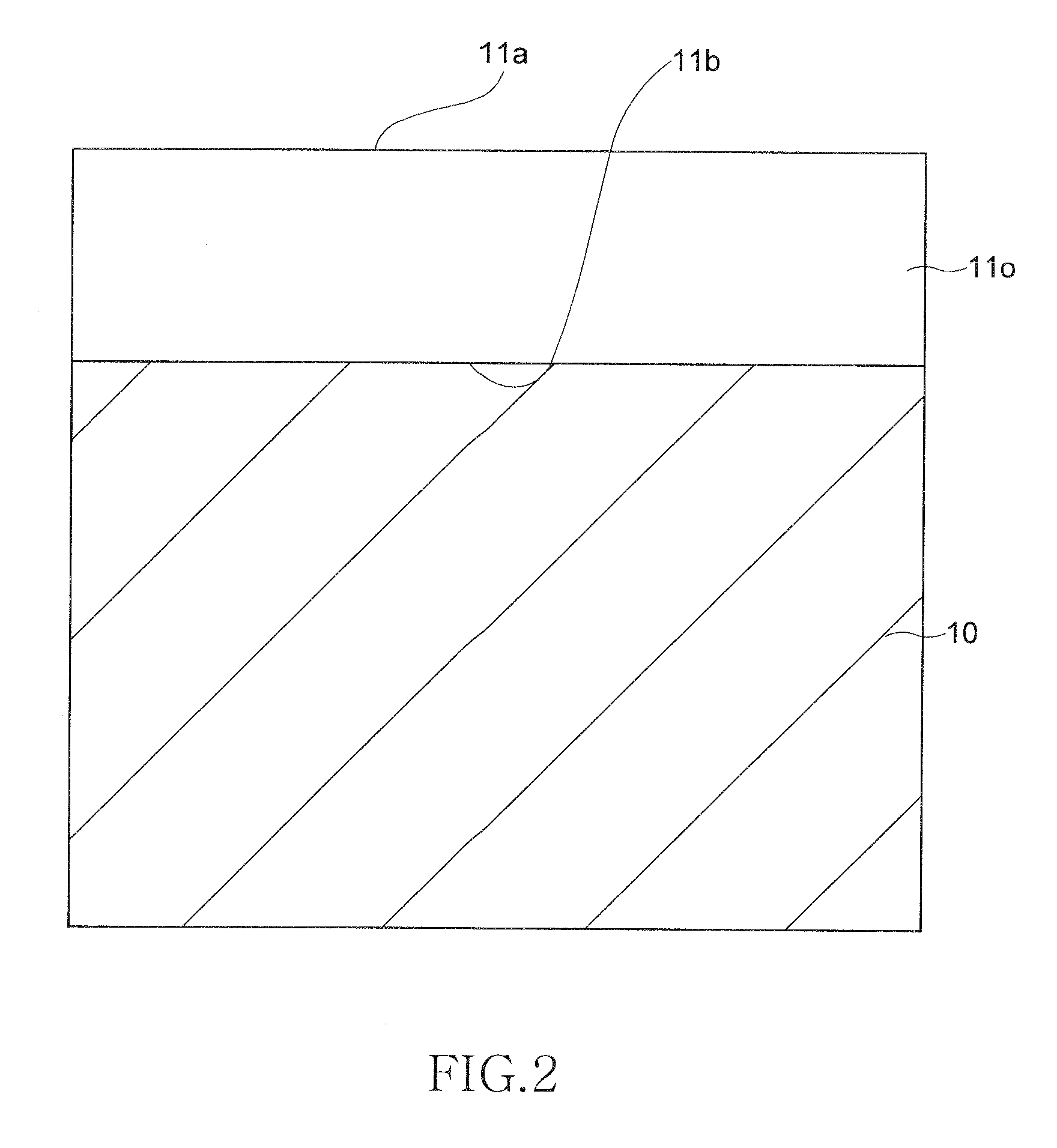
[0027]As shown in FIG. 1, a gate insulating film 11 is formed on a silicon substrate 10. On the gate insulating film 11, a gate electrode 12 made of polysilicon containing boron (B) is formed.

[0028]The gate insulating film 11 contains silicon (Si) atoms, oxygen (O) atoms, nitrogen (N) atoms, and fluorine (F) atoms. Almost all silicon dangling bonds on a surface (top surface) of the gate insulating film 11 are terminated with nitrogen atoms. Almost all silicon dangling bonds on a bottom surface of the gate insulating film 11 contacting the silicon substrate 10 are terminated with fluorine atoms.

[0029]Because of the above configuration, even if a thermal load obtained when, for example, the semiconductor device is he...


PUM


Abstract

Top and bottom surfaces of a gate insulating film are terminated with fluorine atoms and the top surface of the gate insulating film is then etched. New dangling bonds are formed on the top surface of the gate insulating film. Such new dangling bonds are terminated with nitrogen atoms. A semiconductor device is thus obtained that has a silicon substrate and a gate insulating film formed on the silicon substrate and that almost all dangling bonds on the top surface of the gate insulating film are terminated with nitrogen atoms and almost all dangling bonds on the bottom surface contacting the silicon substrate are terminated with fluorine atoms.

Description

TECHNICAL FIELD[0001]The present invention relates to a semiconductor device and a manufacturing method thereof, and, more particularly relates to a semiconductor device that has a gate insulating film containing nitrogen and a manufacturing method thereof.BACKGROUND OF THE INVENTION[0002]Recently, dual gate CMOS transistors have been usually utilized because of semiconductor devices with higher performance and reduced drive voltages. In the dual gate configuration, a gate electrode containing N-type polysilicon to which an N-type impurity (phosphorous, etc.) is introduced is used for the gate electrode of an N-channel transistor. A gate electrode containing P-type polysilicon to which a P-type impurity (boron, etc.) is introduced is used for a P-channel transistor.[0003]If a thermal load is applied to the dual gate CMOS transistor during steps after the gate electrodes are formed, boron in the gate electrode of the PMOS transistor can pass through a gate insulating film made of a s...

Claims


Application Information

Patent Timeline
IPC IPC(8): H01L29/78H01L21/425
CPCH01L21/265H01L21/28185H01L21/28202H01L29/518
Inventor WAKABAYASHI, RYO
Owner ELPIDA MEMORY INC
Why Eureka
Try Eureka