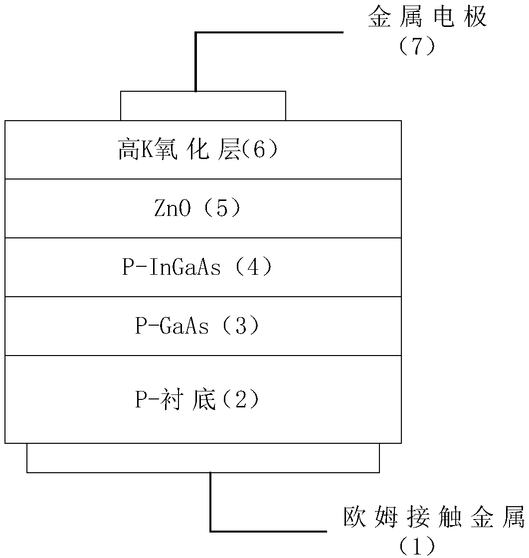
MOS (metal oxide semiconductor) capacitor with high K/ZnO content and low In ingredient InGaAs content and fabrication method
A capacitor and oxide layer technology, applied in the field of microelectronics, can solve problems such as hindering the development of InGaAs devices, capacitance dispersion in the accumulation area, and increased hysteresis voltage, so as to improve the Fermi level pinning effect, reduce power consumption, Effect of Reducing Gate Leakage
- Summary
- Abstract
- Description
- Claims
- Application Information
AI Technical Summary
Problems solved by technology
Method used
Image

Examples
Embodiment 1
[0032] Embodiment 1, making high K oxide is Al 2 o 3 , the channel layer is In with a thickness of 15nm 0.2 Ga 0.8 As, the substrate is a GaAs MOS capacitor.
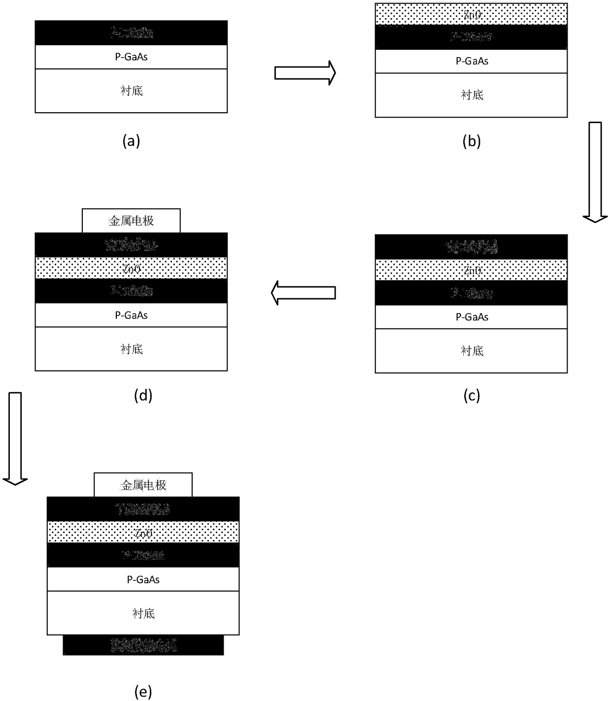
[0033] In step 1, pretreatment is performed on the epitaxial material including the P-type substrate, the P-type GaAs buffer layer and the P-type InGaAs channel layer, as shown in 2(a).
[0034] 1.1) Degrease the epitaxial material sample in acetone and isopropanol, and then rinse it with deionized water;
[0035] 1.2) Soak the rinsed sample in a 1% HF solution for 60 seconds to remove the intrinsic oxide on the surface, then soak it in ammonium sulfide solution for 20 minutes, rinse it with deionized water after taking it out, and put it under N 2 Dry in atmosphere.
[0036] Step 2, depositing a ZnO passivation layer, such as figure 2 (b).
[0037] The pretreated epitaxial material sample was deposited 1nm thick ZnO by atomic layer deposition ALD process, and the deposition process parameters were: the precurso...
Embodiment 2
[0048] Embodiment 2, making high K oxide is ZrO 2 , the channel layer is 30nm thick In 0.2 Ga 0.8 As, the substrate is a MOS capacitor of InP.
[0049] In step 1, pretreatment is performed on the epitaxial material including the P-type substrate, the P-type GaAs buffer layer and the P-type InGaAs channel layer.
[0050] The specific realization of this step is the same as step 1 of embodiment 1
[0051] Step 2, using the atomic layer deposition ALD process, that is, the precursors are DEZn and H 2 O, a 3nm thick ZnO passivation layer was deposited on the pretreated epitaxial material sample at a temperature of 200°C.
[0052] Step 3, using the atomic layer deposition ALD process, that is, the precursors are zirconium tetradimethylamide and H 2 O, the temperature is 200°C. Under the condition of ZnO passivation layer deposited 5nm thick ZrO 2 oxide layer.
[0053] Step 4, will deposit ZrO 2 The sample after the oxidation layer was placed in an annealing furnace with a te...
Embodiment 3
[0057] Embodiment 3, making high K oxide is Al 2 o 3 , the channel layer is 20nm thick In 0.3 Ga 0.7 As, the substrate is a GaSb MOS capacitor.
[0058] In step A, the epitaxial material including the P-type substrate, the P-type GaAs buffer layer and the P-type InGaAs channel layer is pretreated.
[0059] The specific realization of this step is the same as step 1 of embodiment 1
[0060] Step B, depositing a ZnO passivation layer.
[0061] The pretreated epitaxial material sample, the precursor is DEZn and H 2 O, a 5nm thick ZnO passivation layer was deposited under the process conditions of 200°C.
[0062] Step C, depositing Al 2 o 3 oxide layer.
[0063] On the upper surface of the ZnO passivation layer, the atomic layer deposition ALD process is adopted, that is, the precursors are TMA and H 2 O, deposited 5nm thick Al at 200°C 2 o 3 oxide layer.
[0064] Step D, post-deposition annealing.
[0065] will deposit Al 2 o 3 The sample after the oxidation layer...
PUM
 Abstract
Description
Claims
Application Information
 - R&D
- Intellectual Property
- Life Sciences
- Materials
- Tech Scout
- Unparalleled Data Quality
- Higher Quality Content
- 60% Fewer Hallucinations
Browse by: Latest US Patents, China's latest patents, Technical Efficacy Thesaurus, Application Domain, Technology Topic, Popular Technical Reports.
© 2025 PatSnap. All rights reserved.Legal|Privacy policy|Modern Slavery Act Transparency Statement|Sitemap|About US| Contact US: help@patsnap.com