Methods of fabricating field effect transistors including titanium nitride gates over partially nitrided oxide and devices so fabricated

a technology of field effect transistor and titanium nitride, which is applied in the direction of semiconductor devices, basic electric elements, electrical equipment, etc., can solve the problems of poor performance relative to standard cmos, and the failure of major cmos companies, so as to increase the density of the interface state or gate leakage, and improve the reliability

Inactive Publication Date: 2012-10-18
THUNDERBIRD TECH
View PDF3 Cites 0 Cited by
  • Summary
  • Abstract
  • Description
  • Claims
  • Application Information

AI Technical Summary

Benefits of technology

[0006]Fabrication methods according to various embodiments of the invention can provide one or two anneal steps that can permit the production of high-quality TiN (or other nitrided metal) gates over thin PNO dielectrics without the need to lower reliability or to increase the interface state density Dil or gate leakage. Gate structures also may be provided as described below.

Problems solved by technology

In the deep sub-micron regime however, the classical implementation of the transistor may result in poor performance relative to standard CMOS.
However, to date these efforts appear to have been unsuccessful at major CMOS companies.

Method used


Image

  • Methods of fabricating field effect transistors including titanium nitride gates over partially nitrided oxide and devices so fabricated
  • Methods of fabricating field effect transistors including titanium nitride gates over partially nitrided oxide and devices so fabricated
  • Methods of fabricating field effect transistors including titanium nitride gates over partially nitrided oxide and devices so fabricated

Examples


Embodiment Construction

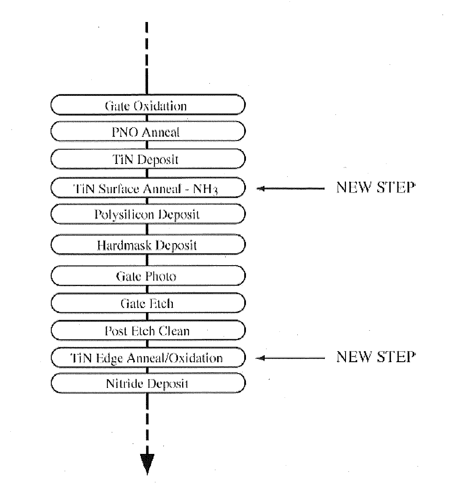
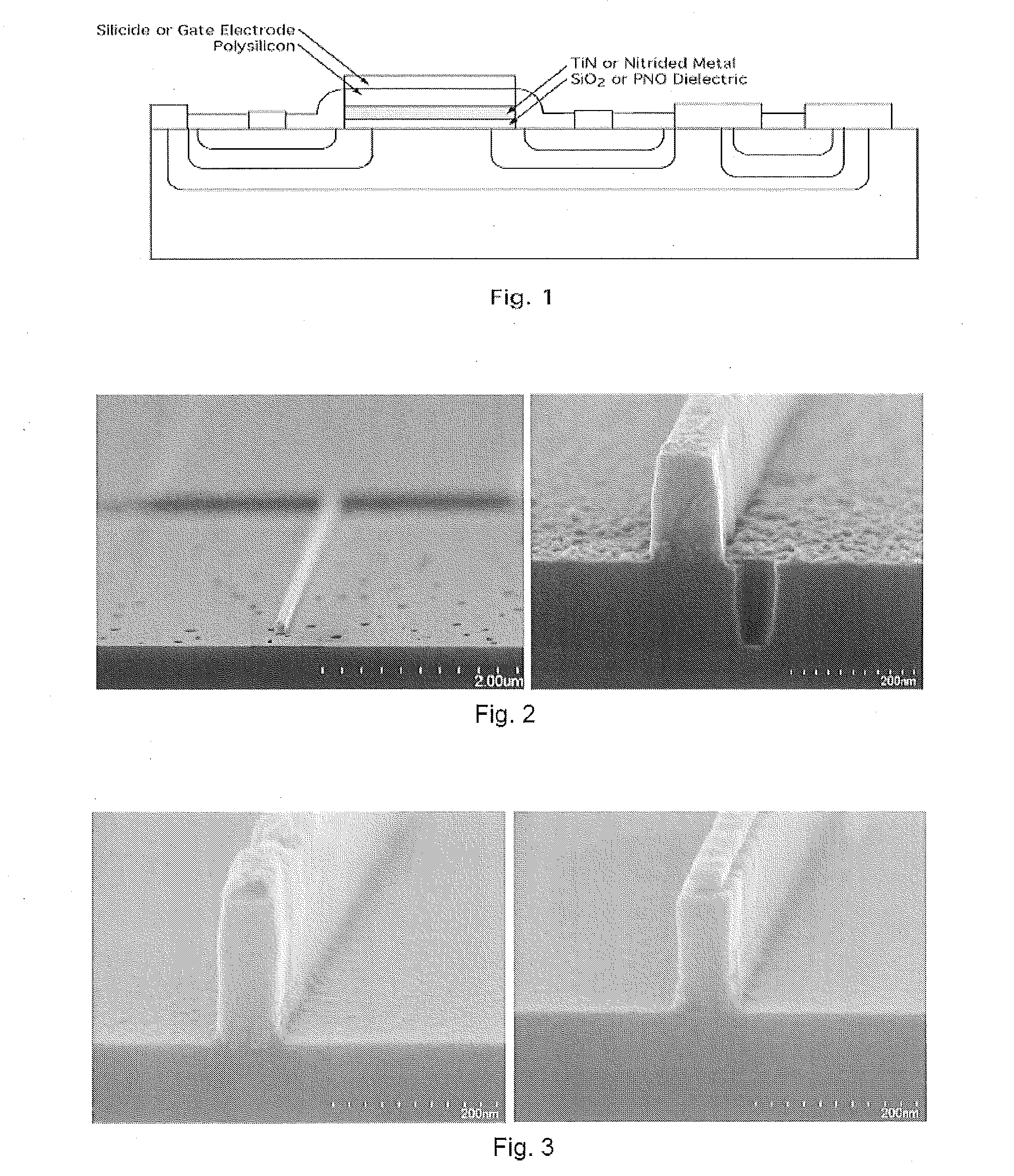
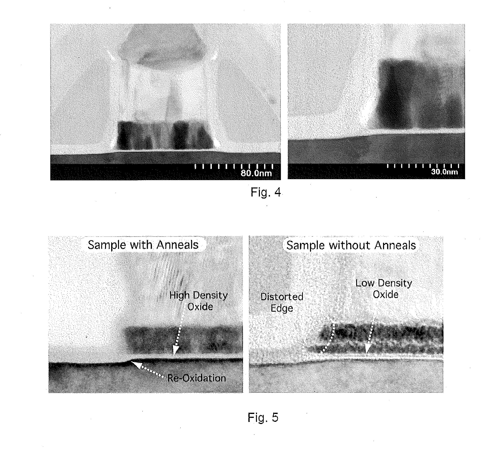
[0016]FIG. 1 illustrates a standard Fermi-FET transistor with a nitrided metal film at the bottom of the gate electrode. A standard MOSFET structure with a nitrided metal film may also be provided in other embodiments. Such a structure has been proposed in the literature, but does not appear to have been realized with high reliability, low trapped charge and / or low dielectric leakage. However, according to various embodiments of the invention, one or more anneals may be performed at specific points in the fabrication process to reduce or eliminate these difficulties and allow the production of nitrided metal gate stacks at quality levels needed by current products.

[0017]One difficulty generally encountered in using nitrided metals in the gate stack is the tendency of the metal atoms to react with the underlying oxide in subsequent high temperature steps, e.g. Rapid Thermal Anneal (RTA) or Spike Anneals, that are used to activate dopant atoms. These defects are shown in FIG. 2, where...


PUM

PropertyMeasurementUnit
thresholdaaaaaaaaaa
threshold voltageaaaaaaaaaa
work functionaaaaaaaaaa

Abstract

A gate of an integrated circuit field effect transistor is fabricated by fabricating a gate insulating layer on an integrated circuit substrate, fabricating a metal nitride layer on the gate insulating layer, annealing the metal nitride layer in a nitridizing ambient and fabricating a cap on the metal nitride layer that has been annealed. Thereafter, the cap on the metal nitride layer may be etched to expose sidewalls thereof and another anneal in a nitridizing ambient may take place. Related integrated circuit field effect transistors are also described.

Description

CROSS REFERENCE TO RELATED APPLICATION[0001]This application claims the benefit of provisional Application No. 61 / 115,841, filed Nov. 18, 2008, entitled Field Effect Transistors Including Titanium Nitride (TiN) Gates Over Partially Nitrided Oxide (PNO) and Methods of Fabricating Same, the disclosure of which is hereby incorporated herein by reference in its entirety as if set forth fully herein.BACKGROUND OF THE INVENTION[0002]This invention relates to integrated circuit devices and fabrication methods and, more particularly, to integrated circuit field effect transistors and fabrication methods therefor.[0003]Field Effect Transistors (FETs), often referred to as Metal Oxide Semiconductor FETs (MOSFETs), MOS devices and / or Complementary MOS (CMOS) devices, are widely used in integrated circuit devices, including logic, memory, processor and other integrated circuit devices. One widely investigated FET is the Fermi-FET, that is described, for example, in U.S. Pat. Nos. 4,984,043; 4,9...

Claims


Application Information

Patent Timeline
Patent Type & Authority Applications(United States)
IPC IPC(8): H01L21/3213
CPCH01L21/28088H01L21/324H01L29/7838H01L29/7833H01L29/4966
Inventor DENNEN, MICHAEL W.
Owner THUNDERBIRD TECH
Why Eureka
Try Eureka