Flip-chip substrate and flip-chip bonding process thereof

a technology of flip-chip substrate and flip-chip bonding, which is applied in the direction of sustainable manufacturing/processing, printed circuit manufacturing, final product manufacturing, etc., can solve the problems of poor reliability of electrical connection large thermal expansion coefficient between the chip and the substrate, etc., and achieve the effect of improving the yield rate of reliability testing

Inactive Publication Date: 2005-12-22
CHEN YU WEN +2
View PDF2 Cites 9 Cited by
  • Summary
  • Abstract
  • Description
  • Claims
  • Application Information

AI Technical Summary

Benefits of technology

[0009] Accordingly, one object of the present invention is to provide a flip-chip substrate and a flip-chip bonding process thereof such that contact pads (cavities) on the substrate are able to align properly with corresponding bonding pads (bumps) on the chip at the melting point of the bump. Ultimately, a good bondage is formed between the chip and the substrate so that the yield rate of reliability testing is improved.

Problems solved by technology

However, the coefficient of thermal expansion between a chip and a substrate is usually large.
Consequently, reliability of electrical connection between the chip and the substrate is poor.

Method used


Image

  • Flip-chip substrate and flip-chip bonding process thereof
  • Flip-chip substrate and flip-chip bonding process thereof
  • Flip-chip substrate and flip-chip bonding process thereof

Examples


Embodiment Construction

[0017] Reference will now be made in detail to the present preferred embodiments of the invention, examples of which are illustrated in the accompanying drawings. Wherever possible, the same reference numbers are used in the drawings and the description to refer to the same or like parts.

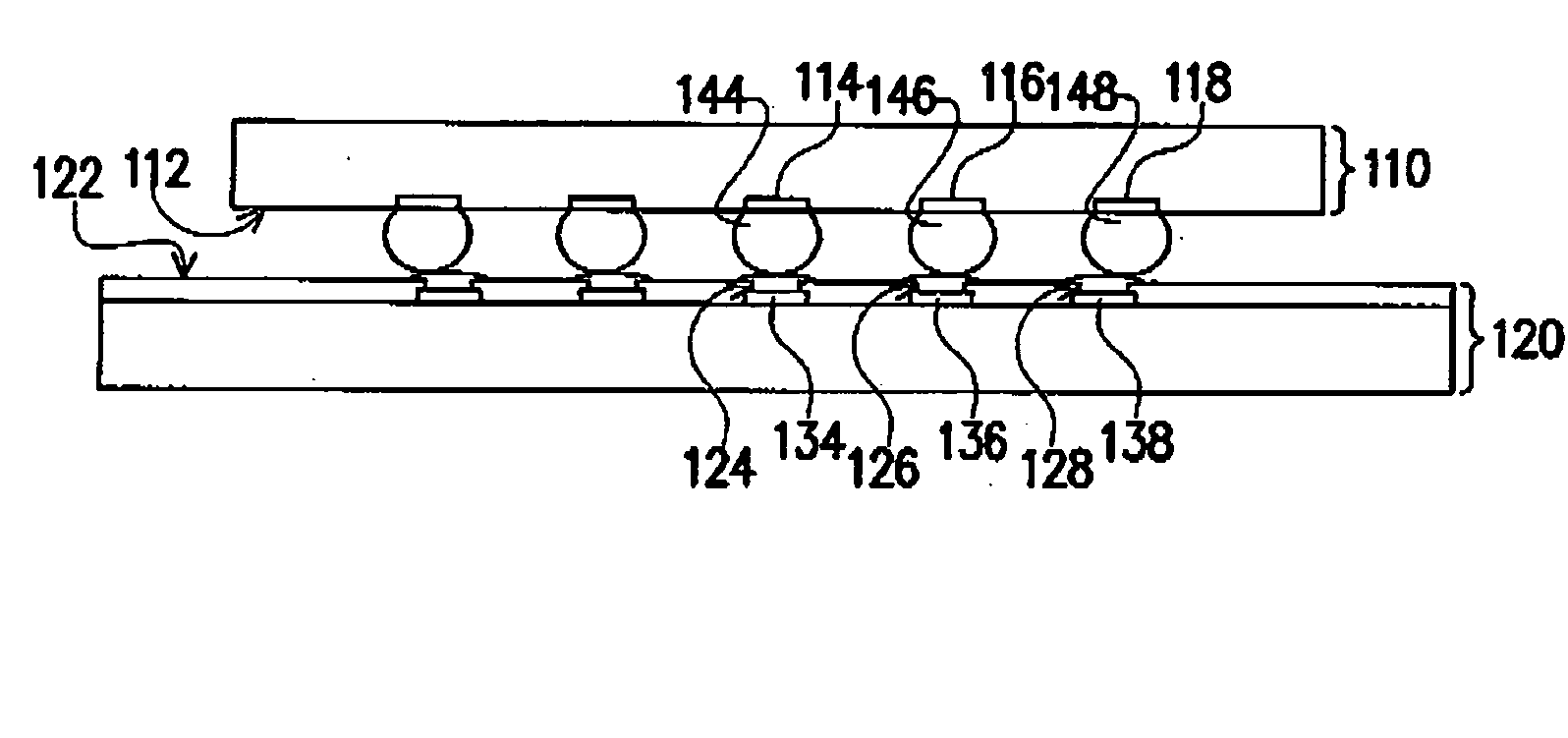
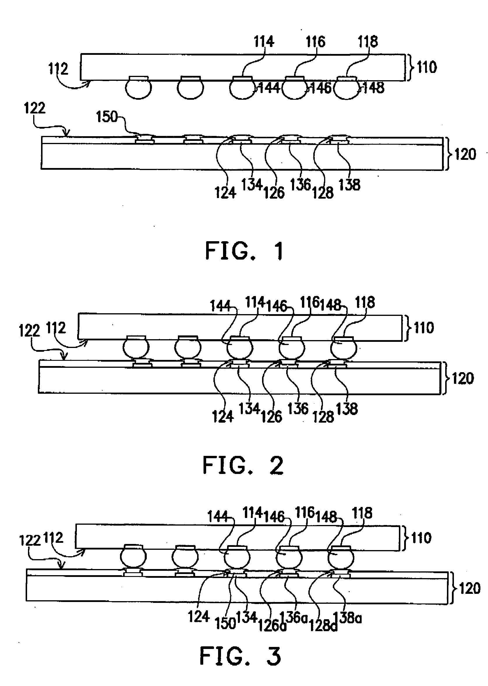
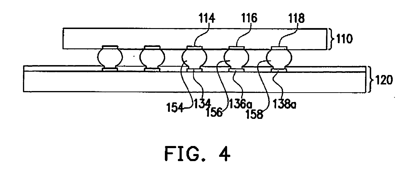
[0018] FIGS. 1 to 4 are schematic cross-sectional views showing the steps for fabricating a flip-chip package according to one preferred embodiment of this invention. In particular, FIG. 1 is a cross sectional view showing a flip-chip substrate and a chip at room temperature. As shown in FIG. 1, a chip 100 having an active surface 112 with a plurality of bonding pads such as 114, 116 and 118 thereon is provided. Furthermore, each bonding pad (114, 116, 118) has a corresponding bump (144, 146, 148). In this embodiment of the invention, the bonding pads 114, 116, 118 and their corresponding bumps 144, 146, 148 are arranged into an array format, for example. The bonding pad 114 (bump 144) located at t...


PUM


Abstract

A flip-chip substrate for bonding with a chip is provided. The chip has an active surface with a plurality of bonding pads and each bonding pad has a bump thereon. The flip-chip substrate has a plurality of contact pads that correspond in positions with the bonding pads on the chip such that the chip pads are aligned to their corresponding contact pads at the melting point of the bump material.

Description

CROSS-REFERENCE TO RELATED APPLICATION [0001] This application is a continuation of a prior application Ser. No. 10 / 605,215, filed Sep. 16, 2003, which claims the priority benefit of Taiwan application serial no. 91136481, filed Dec. 18, 2002.BACKGROUND OF THE INVENTION [0002] 1. Field of Invention [0003] The present invention relates to a flip-chip substrate. More particularly, the present invention relates to a flip-chip substrate and a flip-chip bonding process thereof having the capacity to improve bonding reliability between the chip and the substrate. [0004] 2. Description of Related Art [0005] In the manufacturing of semiconductors, integrated circuits (IC) can be roughly divided into three major fabrication stages, namely, fabrication of a raw die, fabrication of IC on the die to form an IC chip and packaging the IC chip inside a package. The raw die fabrication stage includes fabricating silicon wafer. The IC fabrication stage includes designing circuits, producing various ...

Claims


Application Information

Patent Timeline
Patent Type & Authority Applications(United States)
IPC IPC(8): H01L21/60H05K3/34
CPCH01L24/81H01L2224/81801H01L2924/14H05K3/3436H01L2924/014H05K2203/048H05K2203/1476H01L2924/01033H05K3/3494Y02P70/50
Inventor CHEN, YU-WENHO, MING-LUNLEE, CHUN-YANG
Owner CHEN YU WEN
Why Eureka
Try Eureka