"Machine for removing surfaces of semiconductors and particularly surfaces with integrated circuits"
Inactive Publication Date: 2008-12-11
HELIOS TECH
View PDF13 Cites 12 Cited by
Summary
Abstract
Description
Claims
Application Information
AI Technical Summary
This helps you quickly interpret patents by identifying the three key elements:
Problems solved by technology
Method used
Benefits of technology
Benefits of technology
[0013]The aim of the present invention is to provide a machine for removing surfaces of semiconductors, particularly of surfaces of integrated circuits, which is capable of obviating the drawbacks shown by the described techniques and by known types of machine.
[0014]Within this aim, an object of the present invention is to provide a machine for removing surfaces of semiconductors which eliminates every trace of the integrated circuits from the surface of a semiconductor wafer, rendering impossible any copying or reconstruction attempt by third parties.
[0016]Another object of the present invention is to provide a machine which can be programmed to operate automatically and therefore can be managed even by a small number of operators with limited qualification.
Problems solved by technology
Each new IC, as mentioned, gives rise to intellectual and / or industrial property rights, which during the disposal of the product which has not been used or has been discarded cause problems linked to the need to make it impossible for unlicensed third parties to copy and reproduce the content of said unused integrated circuits.
This grinding operation entails two kinds of risk: a first risk linked to the loyalty of the authorized personnel, and a second more tangible one linked to the fact that pulverization does not always reduce the circuits to a size which makes them unusable; in some cases, it is in fact possible to reconstruct even from microscopic grains of a microchip the intellectual property that it bears.
Further, grinding causes the loss of all the wafer of silicon or other equivalent semiconductor on which the circuits are provided, with a useless waste of raw material.
As an alternative, techniques for the chemical washing of the surfaces of the circuits are known, but they have proved to be very complicated and expensive in terms of machinery, in terms of disposal of the solvents used, and in terms of labor.
Method used
Image
Click on the blue label to locate the original text in one second.
Reading with bidirectional positioning of images and text.
Examples
first embodiment
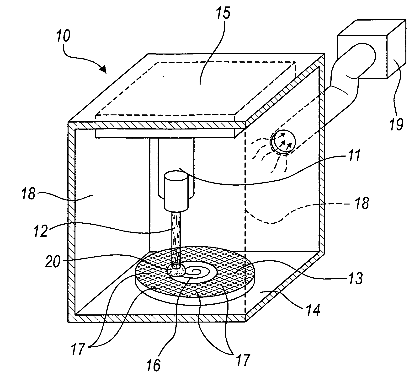
[0027]With reference to the figures, a machine for removing surfaces of semiconductors, particularly surfaces with integrated circuits, according to the invention, is generally designated by the reference numeral 10 in its first embodiment, shown schematically in FIG. 1.
[0028]The machine 10 comprises laser emitter means 11, the at least one beam 12 of which is designed to strike an underlying semiconductor wafer 13 for the ablation of a surface layer 14 having a preset thickness A.
[0029]In this first embodiment, which as mentioned is a non-limiting example of the invention, the emitter means 11, described more clearly hereinafter, emit a single laser beam 12.
[0030]The machine 10 is intended to process a single wafer 13 or a fragment thereof; the wafers 13 can in fact also occur in broken or partly crumbled form.
[0031]The machine 10 further comprises supporting means for said at least one wafer 13 or fragment thereof, for example a supporting surface 14.
[0032]The machine 10 further c...
second embodiment
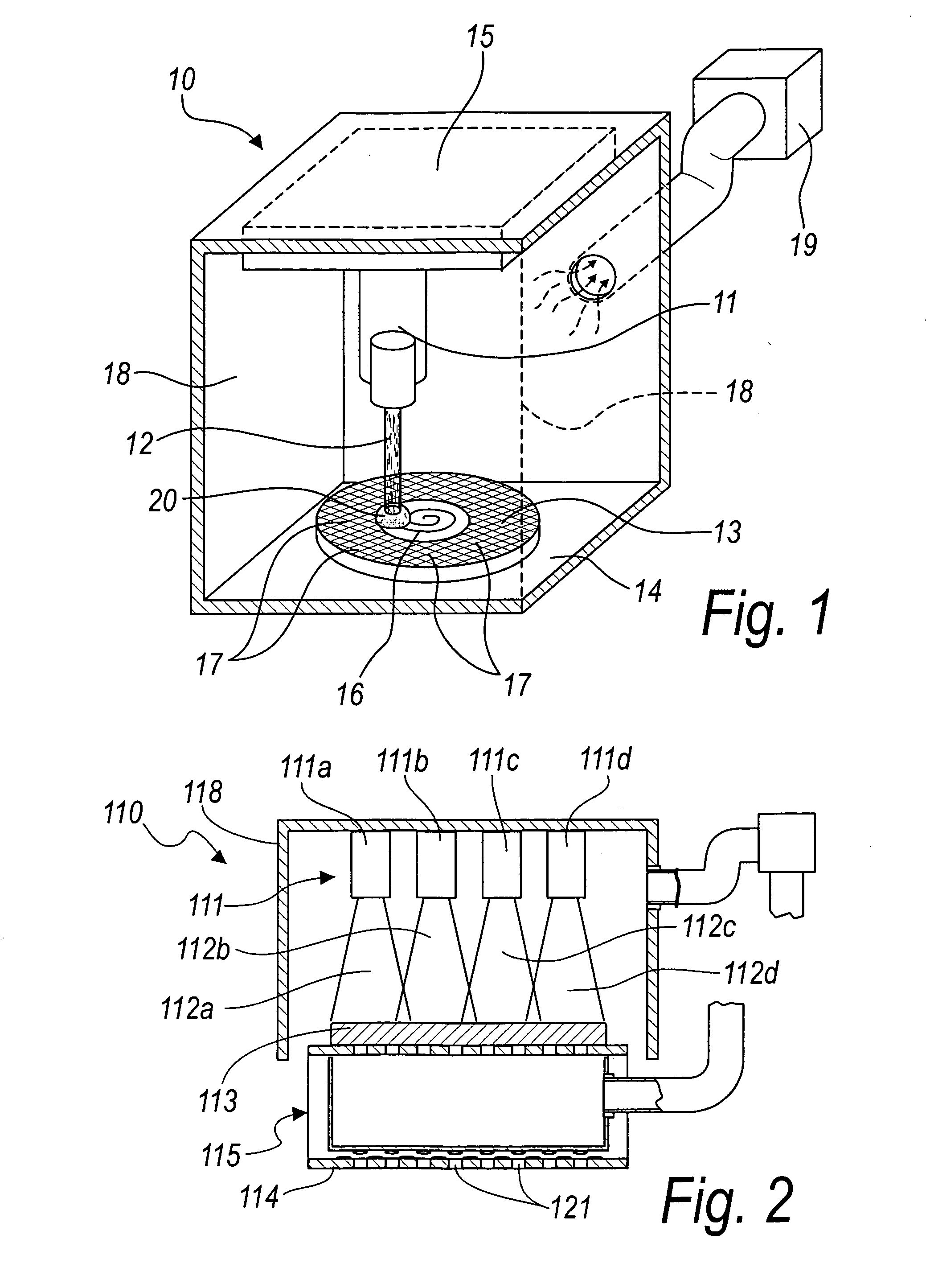
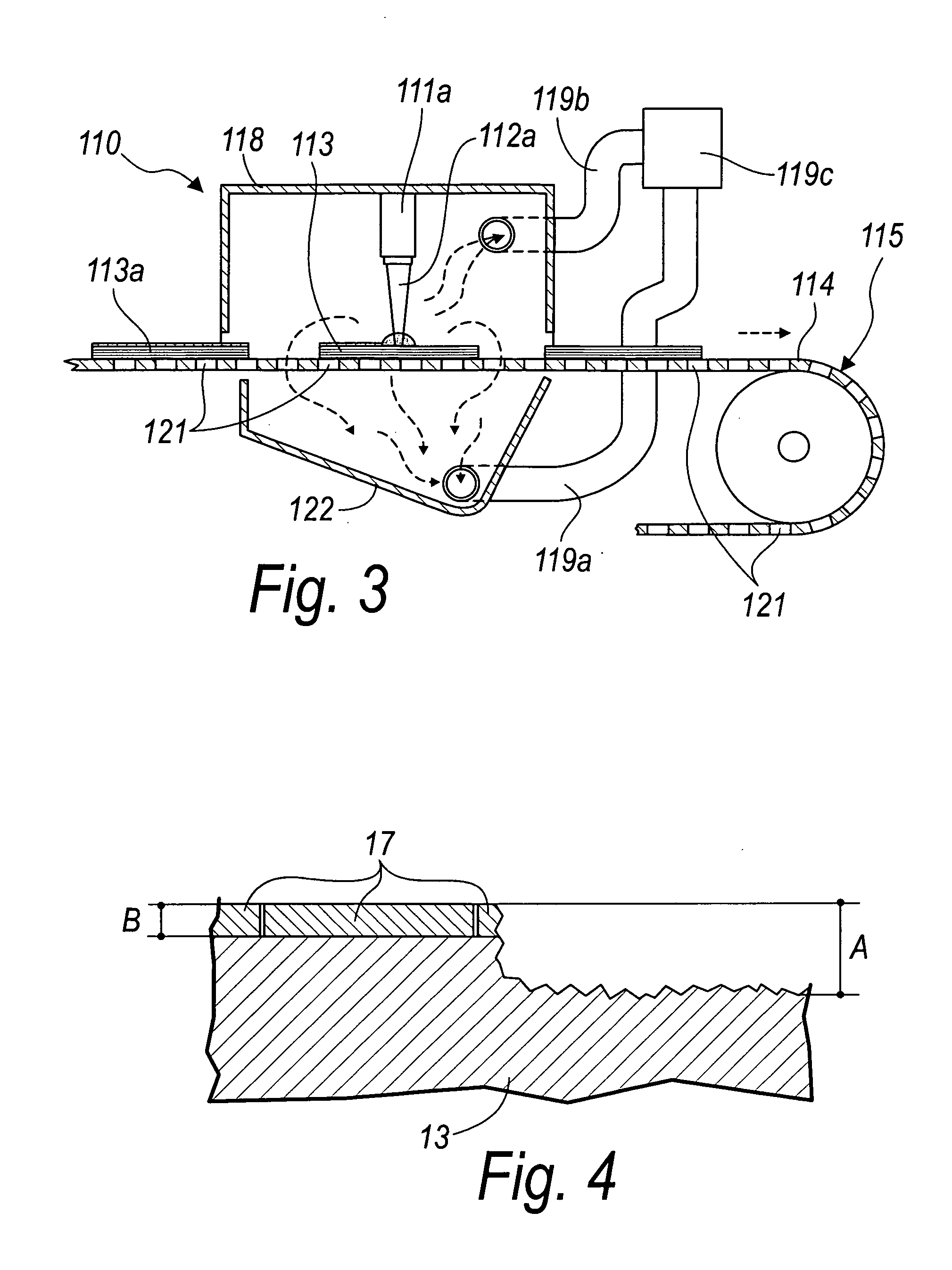
[0053]In its second embodiment, shown schematically in FIGS. 2 and 3 and designated therein by the reference numeral 110, the machine according to the invention is provided with laser emitter means 111, which comprise a series of emitters arranged side by side, which in the described example are four, respectively 111a, 111b, 111c and 111d.
[0054]The respective beams 112a, 112b, 112c and 112d overlap the beam produced by the laterally adjacent emitter, so as to work safely without the risk that regions of the surface being processed might remain unetched by the action of the lasers.
[0055]The beams 112a onward therefore affect as a whole a band of such size as to affect the wafer 113 to be processed along its entire width.
[0056]The emitters 111a onward are arranged side by side in a perpendicular direction with respect to a conveyor belt 114, which forms the supporting surface for a series of subsequent wafers 113, 113a or a fragment thereof, which are loaded onto the belt 114.
[0057]...
PUM
Property
Measurement
Unit
Fraction
aaaaa
aaaaa
Area
aaaaa
aaaaa
Frequency
aaaaa
aaaaa
Abstract
A machine for removing surfaces of semiconductors with integrated circuits, comprising laser emitters, at least one beam of which strikes at least one semiconductorwafer or at least one fragment thereof, for ablation of a surface layer of preset thickness, supports for the at least one wafer or fragment thereof, and movers for the relative movement of the emitters with respect to the at least one wafer or fragment thereof, the movers being adapted to make the emitters follow a path such that the at least one beam emitted thereby travels over the entire surface to be removed of the at least one wafer or fragment thereof.
Description
[0001]The present invention relates to a machine for removing surfaces of semiconductors and particularly surfaces with integrated circuits.BACKGROUND OF THE INVENTION[0002]An integrated circuit or chip is an electronic device constituted by the integration of an electronic circuit on a substrate of semiconductor material (generally silicon, but sometimes also galliumarsenide or other similar and equivalent materials).[0003]The manufacturing cost of an integrated circuit (hereinafter IC) varies little or not at all as its complexity increases, and therefore it is much more economical to develop complex circuits, composed of a series of internal stages which are interconnected to each other and to the outside and centralize all the functions required for a specific apparatus.[0004]For this reason, the microelectronics industry offers a relatively small number of generic ICs but tens of thousands of specialized ICs, each designed for a specific purpose, thus becoming precious company...
Claims
Application Information
Patent Timeline
Application Date:The date an application was filed.
Publication Date:The date a patent or application was officially published.
First Publication Date:The earliest publication date of a patent with the same application number.
Issue Date:Publication date of the patent grant document.
PCT Entry Date:The Entry date of PCT National Phase.
Estimated Expiry Date:The statutory expiry date of a patent right according to the Patent Law, and it is the longest term of protection that the patent right can achieve without the termination of the patent right due to other reasons(Term extension factor has been taken into account ).
Invalid Date:Actual expiry date is based on effective date or publication date of legal transaction data of invalid patent.

