Semiconductor device

a technology of semiconductor devices and semiconductors, applied in semiconductor devices, semiconductor/solid-state device details, electrical apparatus, etc., can solve the problems of reducing the reliability of the semiconductor device with respect to external force, and the inability to take the flexibility of the substrate for various applications, etc., to achieve high reliability, not easily damaged by external force, and high yield

Inactive Publication Date: 2008-12-11
SEMICON ENERGY LAB CO LTD
View PDF31 Cites 92 Cited by
  • Summary
  • Abstract
  • Description
  • Claims
  • Application Information

AI Technical Summary

Benefits of technology

[0007]In view of the foregoing problems, it is an object of the present invention to provide a semiconductor device which can increase reliability with respect to external force, especially pressing force, while the circuit size or the capacity of memory is maintained.
[0008]The present inventors focus attention on a structure body in which a fibrous body of an organic compound or an inorganic compound is impregnated with an organic resin, and have found that reliability of a semiconductor device with respect to external force, especially pressing force, is dramatically increased when an element layer including a semiconductor element formed using a thin semiconductor film is provided between a pair of structure bodies each having a stack of the plurality of fibrous bodies, especially the plurality of fibrous bodies including three or more layers.
[0011]As the fibrous body, a woven fabric or a nonwoven fabric which uses a high-strength fiber of an organic compound or an inorganic compound is used. A high-strength fiber is specifically a fiber with a high tensile modulus of elasticity or a fiber with a high Young's modulus. By using a high-strength fiber for the fibrous body, even when local pressing force is applied to a semiconductor device, the pressure is dispersed throughout the fibrous body; accordingly, partial stretching of the semiconductor device can be prevented. That is, destruction of a wiring, a semiconductor element, or the like, which is caused by the partial stretching, can be prevented.
[0013]According to the present invention, a highly-reliable semiconductor device which is not easily damaged by external force, especially pressing force, can be manufactured with a high yield.

Problems solved by technology

Accordingly, reliability of the semiconductor device with respect to force which is externally applied (external force) is reduced, resulting in a problem in that the above-described advantage in that the substrate having flexibility can be expected to have various applications cannot be sufficiently taken.

Method used


Image

  • Semiconductor device
  • Semiconductor device
  • Semiconductor device

Examples


embodiment mode 1

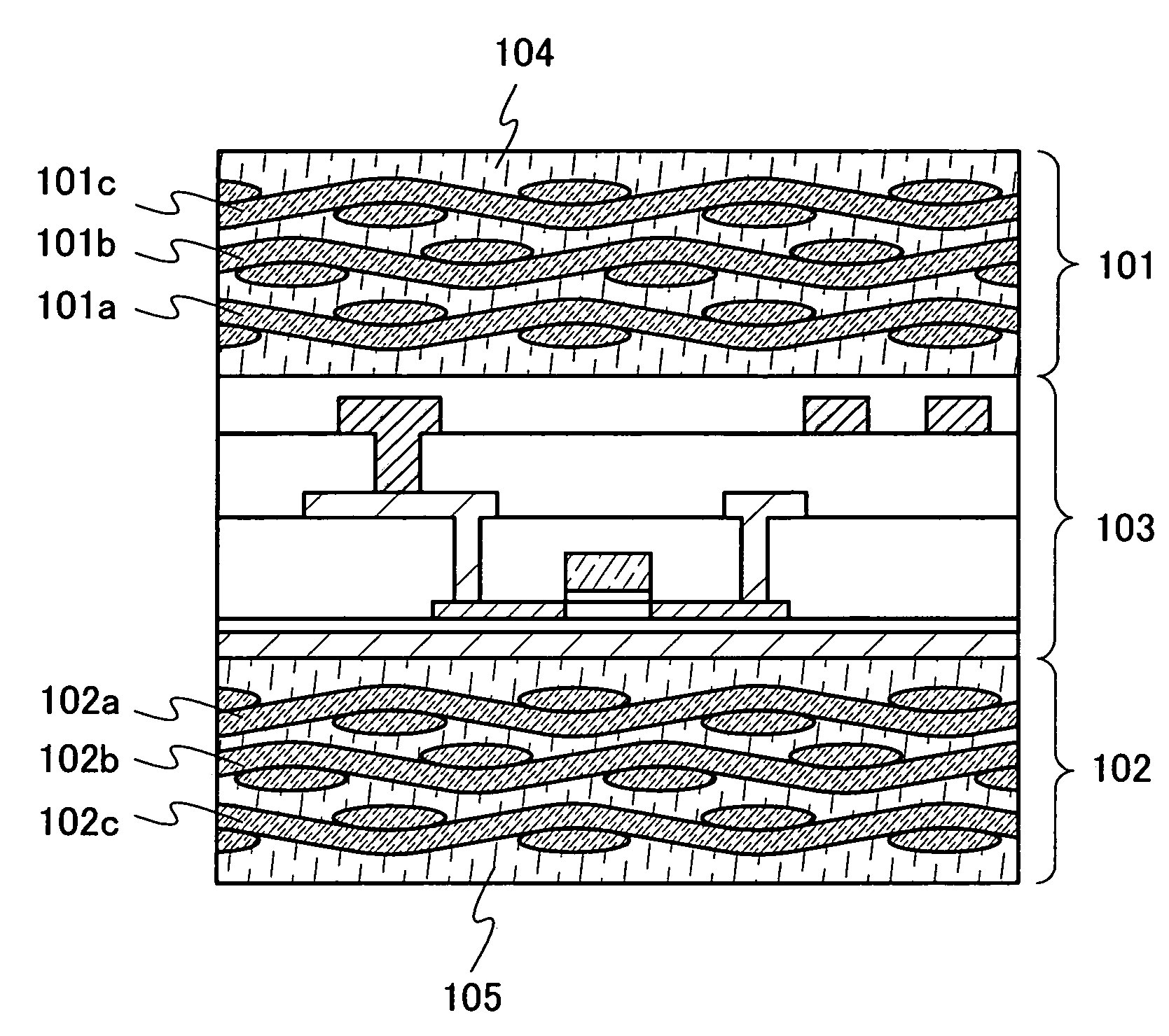
[0042]FIG. 1 shows an example of a cross-sectional view of a semiconductor device of the present invention. The semiconductor device shown in FIG. 1 includes a structure body 101, a structure body 102, and an element layer 103 provided between the pair of structure bodies 101 and 102. The structure body 101 includes a fibrous body 101a, a fibrous body 101b, and a fibrous body 101c each of which is formed from an organic compound or an inorganic compound; and an organic resin 104 with which the fibrous bodies 101a to 101c are impregnated. The fibrous body 101a, the fibrous body 101b, and the fibrous body 101c are stacked. Similarly, the structure body 102 includes a fibrous body 102a, a fibrous body 102b, and a fibrous body 102c each of which is formed from an organic compound or an inorganic compound; and an organic resin 105 with which the fibrous bodies 102a to 102c are impregnated. The fibrous body 102a, the fibrous body 102b, and the fibrous body 102c are stacked.

[0043]Although ...

embodiment mode 2

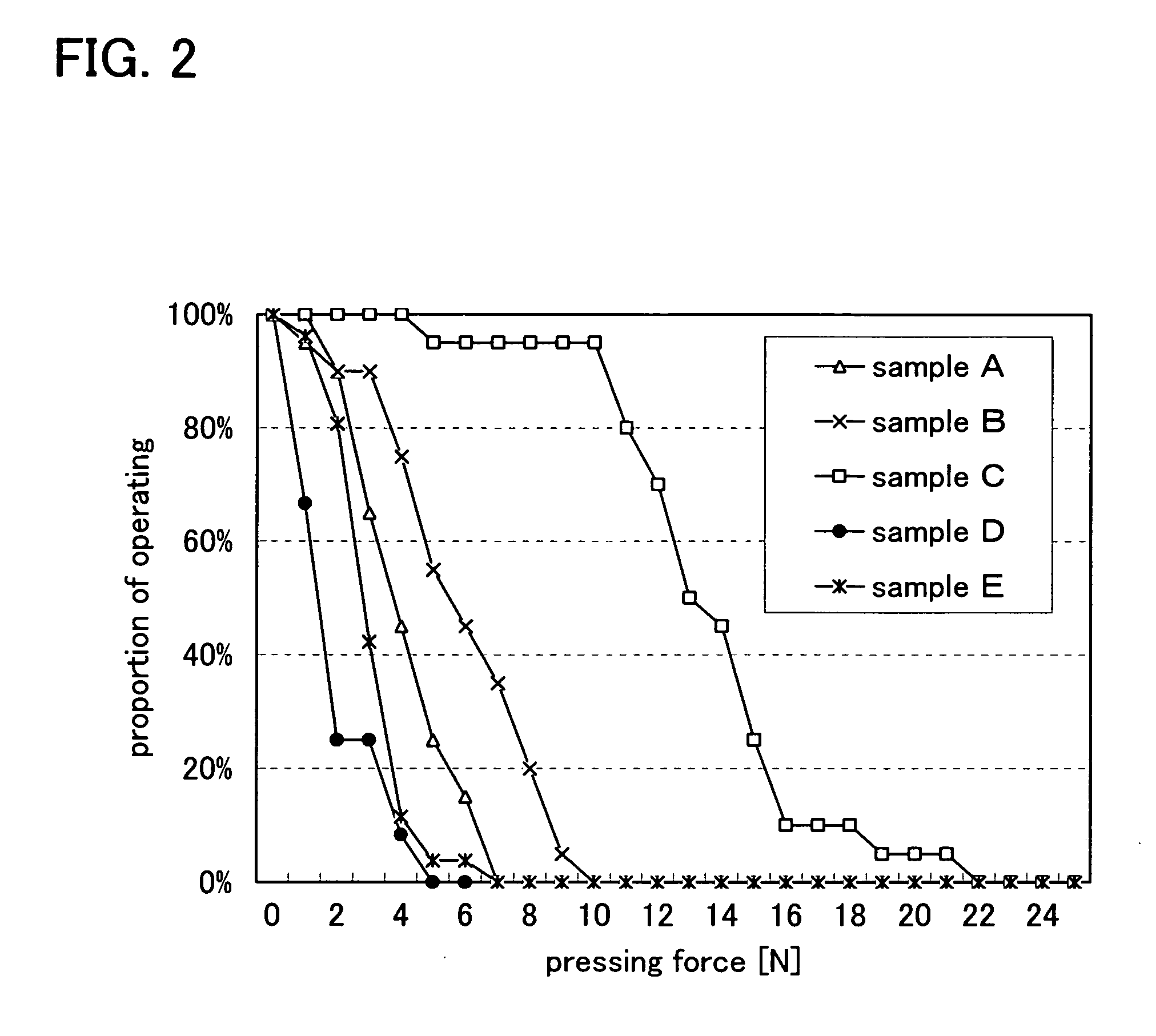
[0063]The proportion of operating semiconductor devices at the time of applying local pressing force with a pen was tested by the present inventors.

[0064]In the test, an RF tag was used as a semiconductor device. It is to be noted that an RF tag is a recording medium used for technique to identify individuals by transmission and reception of signals wirelessly (RFID: radio frequency identification), and signals can be transmitted and received without contact between the RF tag and an interrogator called a reader or a reader / writer. Most of the RF tags are shaped like a card or shaped like a chip with the size smaller than a card; however, the RF tags may be variously shaped.

[0065]The test was conducted on an RF tag in which an element layer was interposed between a pair of prepregs each having a fibrous body of one layer (a sample A), an RF tag in which an element layer was interposed between a pair of prepregs each having fibrous bodies of two layers (a sample B), and an RF tag in ...

embodiment mode 3

[0072]This embodiment mode describes a manufacturing method of a semiconductor device of the present invention. Although this embodiment mode describes a thin film transistor (TFT) as an example of a semiconductor element, a semiconductor element used for a semiconductor device of the present invention is not limited thereto. For example, a memory element, a diode, a resistor, a coil, a capacitor, an inductor, or the like can be used as well as a TFT.

[0073]First, as shown in FIG. 6A, an insulating film 701, a separation layer 702, an insulating film 703, and a semiconductor film 704 are sequentially formed over a substrate 700 having heat resistance. The insulating film 701, the separation layer 702, the insulating film 703, and the semiconductor film 704 can be successively formed.

[0074]As the substrate 700, a glass substrate such as barium borosilicate glass or aluminoborosilicate glass, a quartz substrate, a ceramic substrate, or the like can be used. Alternatively, a metal subst...


PUM


Abstract

To provide a semiconductor device which can increase reliability with respect to external force, especially pressing force, while the circuit size or the capacity of memory is maintained. A pair of structure bodies each having a stack of fibrous bodies of an organic compound or an inorganic compound, which includes a plurality of layers, especially three or more layers, is impregnated with an organic resin, and an element layer provided between the pair of structure bodies are included. The element layer and the structure body can be fixed to each other by heating and pressure bonding. Further, a layer for fixing the element layer and the structure body may be provided. Alternatively, the structure body fixed to an element layer can be formed in such a way that after a plurality of fibrous bodies is stacked over the element layer, the fibrous bodies are impregnated with an organic resin.

Description

BACKGROUND OF THE INVENTION[0001]1. Field of the Invention[0002]The present invention relates to semiconductor devices using substrates having flexibility.[0003]2. Description of the Related Art[0004]A substrate having flexibility has advantages in that mechanical strength with respect to vibration and shock is excellent as compared to a glass substrate, the thickness is easily suppressed, and a degree of freedom in shape is high. Therefore, a semiconductor device using the substrate having flexibility is expected to have various applications. The substrates having flexibility may include a substrate which does not have heat resistance high enough to withstand heat treatment in a manufacturing process of a semiconductor element. For this case, a manufacturing method is proposed in which after a semiconductor element is formed over a substrate having heat resistance which is separately prepared, the semiconductor element is separated from the substrate to be bonded to the substrate h...

Claims


Application Information

Patent Timeline
Patent Type & Authority Applications(United States)
IPC IPC(8): H01L23/29
CPCH01L21/56H01L23/295H01L23/3157H01L2924/12044H01L2924/0002H01L2924/19041H01L2924/00H01L23/14H01L23/18
Inventor OHTANI, HISASHISUGIYAMA, EIJI
Owner SEMICON ENERGY LAB CO LTD
Why Eureka
Try Eureka