Method for manufacturing shallow trench isolation structure

a manufacturing method and technology of isolation structure, applied in the direction of basic electric elements, semiconductor/solid-state device manufacturing, electric apparatus, etc., can solve the problems of increasing cost, reducing reliability of manufacturing process, and complicated manufacturing process, so as to increase uniformity of wafer surface and increase reliability of manufacturing process

Inactive Publication Date: 2008-12-11
UNITED MICROELECTRONICS CORP
View PDF4 Cites 4 Cited by
  • Summary
  • Abstract
  • Description
  • Claims
  • Application Information

AI Technical Summary

Benefits of technology

[0008]Accordingly, at least one objective of the present invention is to provide a complex chemical mechanical polishing process capable of preventing the problems of under polishing or over polishing. Therefore, the uniformity of the wafer surface is increased and the reliability of the manufacturing process is increased as well.
[0009]At least another objective of the present invention is to provide method of forming a shallow trench isolation structure. By using the method of the present invention, the dishing phenomenon can be prevented so as to increase the planarization of the shallow trench isolation structure and the reliability of the manufacturing process.

Problems solved by technology

However, in the STI-CMP process, there still exists some drawbacks comprising, for example, the under polishing issue caused by low selective ratio of oxide to nitride or the dishing phenomenon caused by over polishing.
Hence, the manufacturing process becomes more complicated and the cost is increased as well.
In addition, the STI-CMP process also confronts with the problems of being hard to control the thickness and uniformity of the oxide layer of the STI so that the reliability of the manufacturing process is decreased.

Method used


Image

  • Method for manufacturing shallow trench isolation structure
  • Method for manufacturing shallow trench isolation structure
  • Method for manufacturing shallow trench isolation structure

Examples


Embodiment Construction

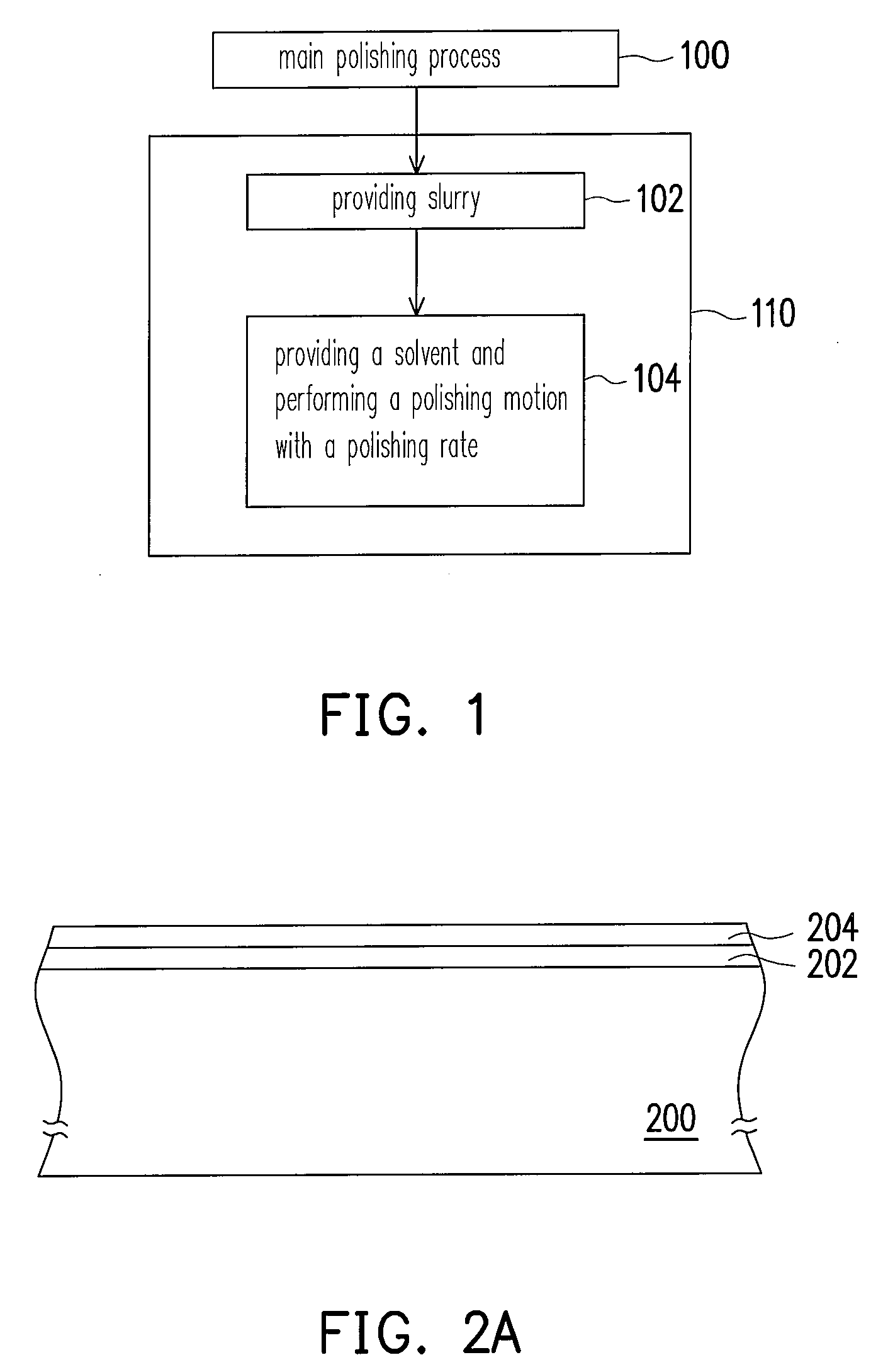
[0018]FIG. 1 is a flowchart illustrating a complex chemical mechanical polishing process according to a preferred embodiment of the invention.

[0019]As shown in FIG. 1, a main polishing process (step 100) is performed. In the main polishing process comprises steps of providing a slurry and performing a polishing motion of a polishing rate V1. The slurry can be, for example, a high selectivity slurry (HSS). The HSS can be, for example, a cerium oxide-contained solution.

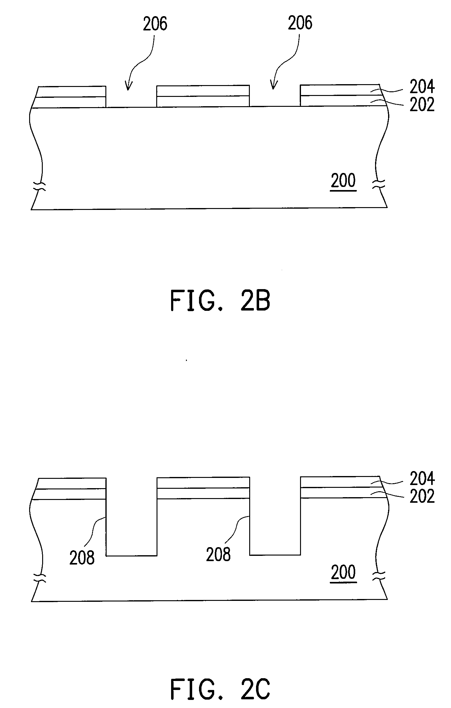
[0020]The main polishing process mentioned above is the same as the conventional chemical mechanical polishing process. The purpose of the main polishing process is to remove most of material which is predetermined to be removed away in a short period of time. In order to increase the polishing rate, the main polishing process is stopped once the interface between the different materials is exposed although some of the material predetermined to be removed away still remain on the wafer.

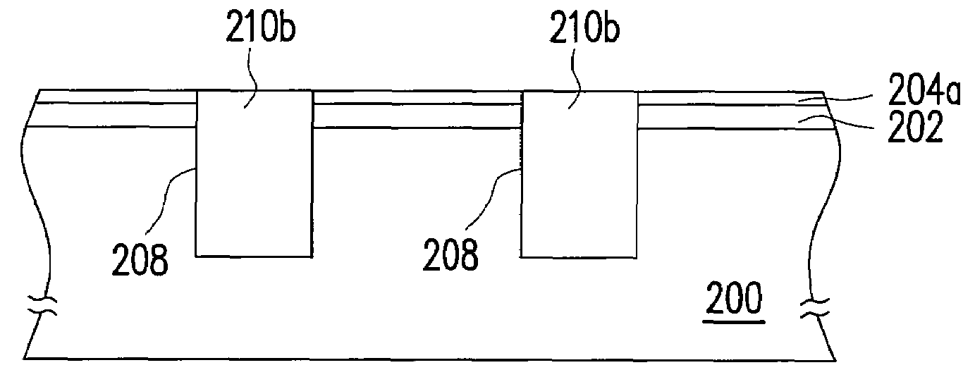
[0021]After the main polishing pro...


PUM


Abstract

A method of forming a shallow trench isolation structure includes steps of providing a substrate having a patterned mask layer formed thereon, wherein a trench is located in the substrate and the patterned mask layer exposes the trench. Thereafter, a dielectric layer is formed over the substrate to fill the trench. Then, a main polishing process with a first polishing rate is performed to remove a portion of the dielectric layer. An assisted polishing process is performed to remove the dielectric layer and a portion of the mask layer. The assisted polishing process includes steps of providing a slurry in a first period of time and then providing a solvent and performing a polishing motion of a second polishing rate in a second period of time. The second polishing rate is slower than the first polishing rate. Further, the mask layer is removed.

Description

CROSS-REFERENCE TO RELATED APPLICATION[0001]This application is a divisional of an application Ser. No. 11 / 465,457, filed on Aug. 18, 2006, now pending. The entirety of the above-mentioned patent applications is hereby incorporated by reference herein and made a part of this specification.BACKGROUND OF THE INVENTION[0002]1. Field of Invention[0003]The present invention relates to a chemical mechanical polishing process. More particularly, the present invention relates to a complex chemical mechanical polishing process.[0004]2. Description of Related Art[0005]In the semiconductor process, with the decrease of the device size, the resolution of the photolithography is increased. Furthermore, with the decrease of the depth of focus, the demand for having a more even surface of the wafer is high.[0006]Currently, the wafer planarization is accomplished by the chemical mechanical polishing (CMP) process. Typically, the CMP process, especially the traditional silica-based shallow-trench-is...

Claims


Application Information

Patent Timeline
Patent Type & Authority Applications(United States)
IPC IPC(8): H01L21/76
CPCH01L21/31053
Inventor CHEN, YEN-CHUCHU, HSIN-KUNTSAI, TENG-CHUNCHEN, CHIA-HSI
Owner UNITED MICROELECTRONICS CORP
Why Eureka
Try Eureka