Check patentability & draft patents in minutes with Patsnap Eureka AI!

Mask ROM device, semiconductor device including the mask ROM device, and methods of fabricating mask ROM device and semiconductor device

a technology of mask rom and semiconductor device, which is applied in the field of mask rom device, semiconductor device including and methods of fabricating the mask rom device and semiconductor device, can solve the problems of high ion implantation energy, difficult to implant ions into the channel region, and difficult to form ion implantation mask patterns at precise locations, etc., to achieve stable output data, low leakage current, and high breakdown voltage

Inactive Publication Date: 2008-12-18
SAMSUNG ELECTRONICS CO LTD
View PDF4 Cites 1 Cited by
  • Summary
  • Abstract
  • Description
  • Claims
  • Application Information

AI Technical Summary

Benefits of technology

[0009]Embodiments exemplarily described herein can be characterized as capable of providing a mask read-only-memory (ROM) device in which a transistor of an on-cell can maintains low leakage current and a sufficiently high breakdown voltage and a transistor of an off-cell can stably output data because no channel is formed even when the transistor is activa...

Problems solved by technology

However, as a design rule of gate electrodes is reduced, it can be very difficult to implant ions into the channel region.
As the channel regions into which ions are implanted are reduced, it becomes more difficult to form ion implantation mask patterns at precise locations.
In addition, because ions penetrate through the gate electrode, high ion implantation energy is required.

Method used


Image

  • Mask ROM device, semiconductor device including the mask ROM device, and methods of fabricating mask ROM device and semiconductor device
  • Mask ROM device, semiconductor device including the mask ROM device, and methods of fabricating mask ROM device and semiconductor device
  • Mask ROM device, semiconductor device including the mask ROM device, and methods of fabricating mask ROM device and semiconductor device

Examples


Embodiment Construction

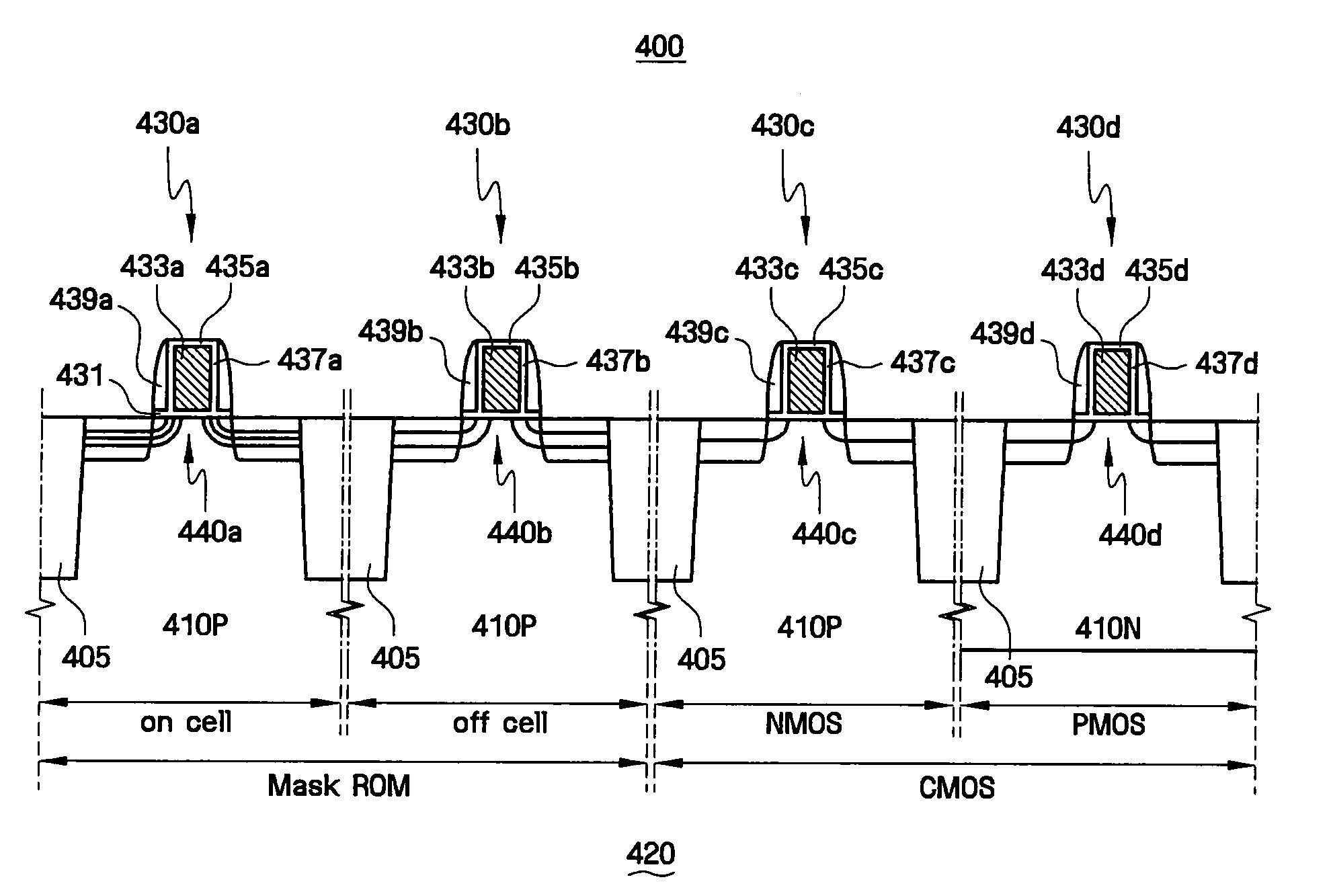
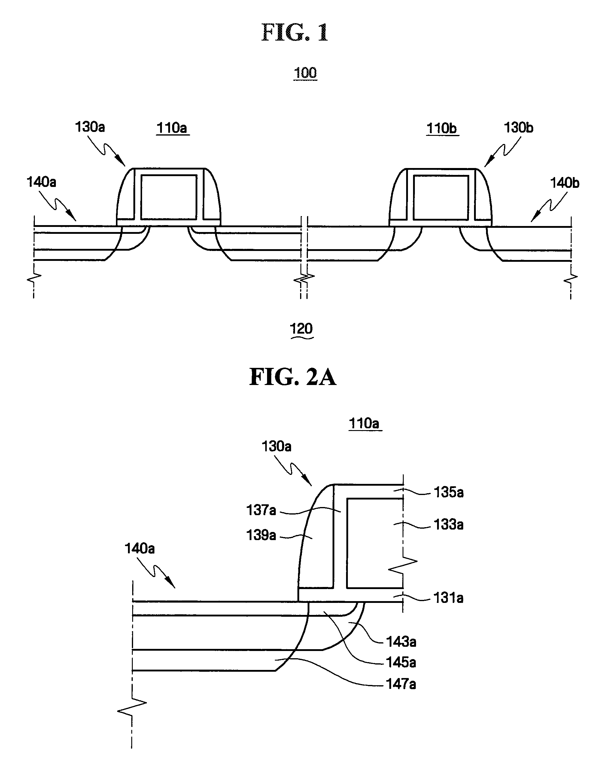
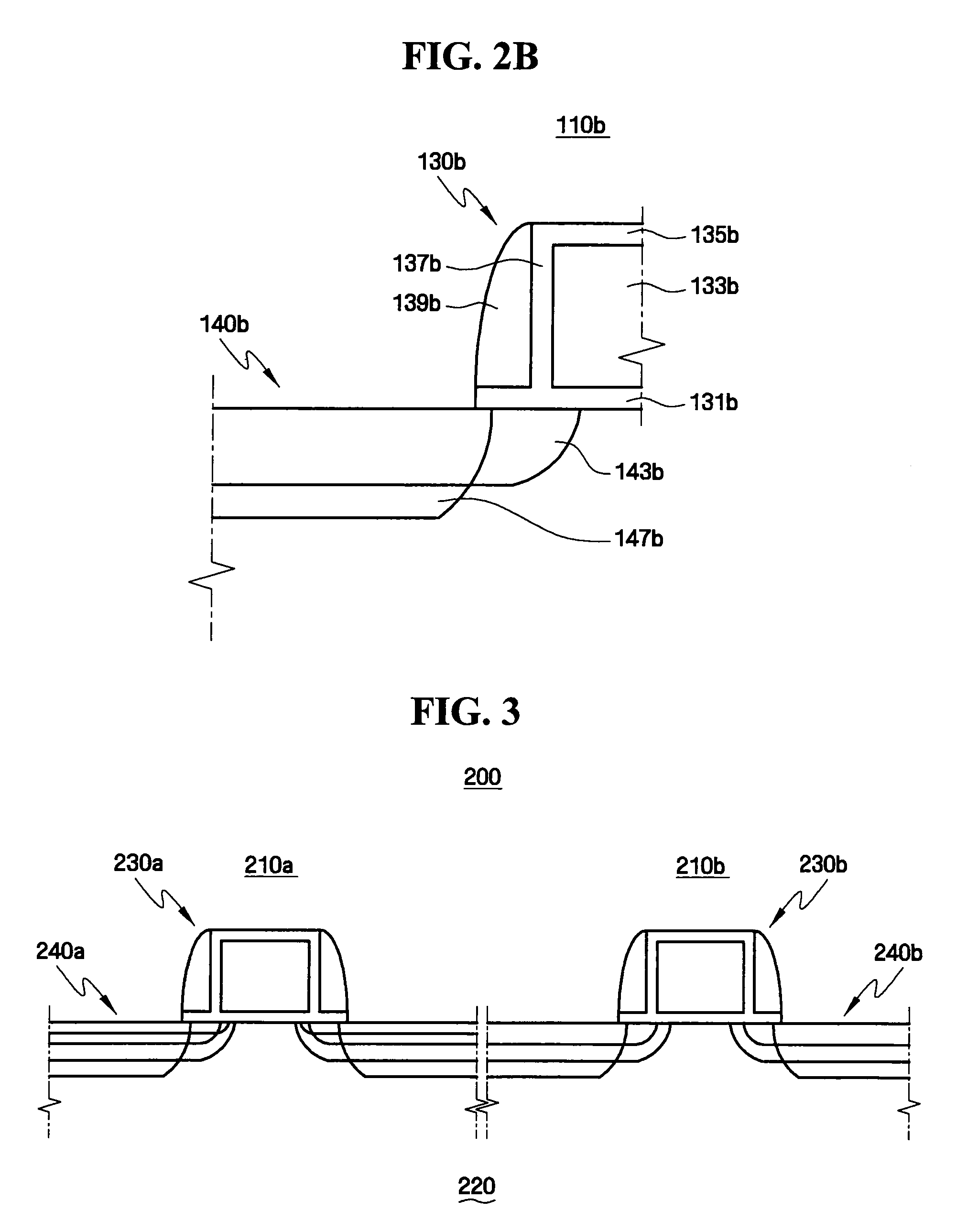
[0022]Exemplary embodiments of the present invention will now be described more fully with reference to the accompanying drawings. These embodiments may, however, be realized in many different forms and should not be construed as being limited to the embodiments set forth herein. Rather, these embodiments are provided so that this disclosure will be thorough and complete, and will fully convey the concept of the invention to those skilled in the art. In the drawings, sizes and relative sizes of the layers and regions are exaggerated for clarity. Like reference numerals in the drawings denote like elements, and thus their description will be omitted.

[0023]Exemplary embodiments of the present invention are described herein with reference to cross-sectional illustrations representing idealized embodiments. As such, variations from the shapes of the illustrations as a result, for example, of manufacturing techniques and / or tolerances, are to be expected. Thus, embodiments of the inventi...


PUM


Abstract

A mask read-only memory (ROM) device, which can stably output data, includes an on-cell and an off-cell. The on-cell includes an on-cell gate structure on a substrate and an on-cell junction structure within the substrate. The off-cell includes an off-cell gate structure on the substrate and an off -cell junction structure within the substrate. The on-cell gate structure includes an on-cell gate insulating film, an on-cell gate electrode and an on-cell gate spacer. The on-cell junction structure includes first and second on-cell ion implantation regions of a first polarity and third and fourth on-cell ion implantation regions of a second polarity. The off-cell gate structure includes an off-cell gate insulating film, an off-cell gate electrode and an off-cell gate spacer. The off-cell junction structure includes first and second off-cell ion implantation regions of the first polarity and a third off-cell ion implantation region of the second polarity.

Description

[0001]This application claims the benefit of foreign priority to Korean Patent Application No. 10-2007-0057484 filed on Jun. 12, 2007, the disclosure of which is incorporated herein by reference in its entirety.BACKGROUND[0002]1. Field of Invention[0003]Embodiments of the present invention relate generally to mask read-only-memory (ROM) devices, semiconductor devices including mask ROM devices and methods of fabricating the mask ROM devices and semiconductor device including the same. More particularly, embodiments of the present invention relate to a mask ROM device including a cell junction, which has ion implantation regions of opposite polarities and thus enables an on-cell and an off-cell to operate stably, a semiconductor device including such a mask ROM device, and methods of fabricating the mask ROM device and the semiconductor device.[0004]2. Description of the Related Art[0005]Mask read-only-memory (ROM) devices are read-only semiconductor memory devices to which data cann...

Claims


Application Information

Patent Timeline
IPC IPC(8): H01L27/118H01L21/8238
CPCH01L21/26586H01L21/823807H01L21/823814H01L27/105H01L27/11266H01L27/11293H01L27/1052H10B20/387H10B20/65H10B20/00H10B99/00
Inventor LEE, YONG-KYUHAN, JEONG-UKJEON, HEE-SEOGKIM, YOUNG-HOCHUN, MYUNG-JOMOON, JUNG-HO
Owner SAMSUNG ELECTRONICS CO LTD
Features
  • R&D
  • Intellectual Property
  • Life Sciences
  • Materials
  • Tech Scout
  • Unparalleled Data Quality
  • Higher Quality Content
  • 60% Fewer Hallucinations
Learn More