Negative voltage detection circuit for synchronous rectifier mosfet

a synchronous rectifier and detection circuit technology, applied in the direction of efficient power electronics conversion, measurement using ac-dc conversion, instruments, etc., can solve problems such as voltage drop of output voltag

Inactive Publication Date: 2008-12-18
HIMAX TECH LTD
View PDF7 Cites 8 Cited by
  • Summary
  • Abstract
  • Description
  • Claims
  • Application Information

AI Technical Summary

Benefits of technology

[0008]An objective of the present invention is to provide a negative voltage detection circuit for a synchronous rectifier MOSFET, capable of precisely detecting a small negative voltage.

Problems solved by technology

This will adversely result in a voltage drop of the output voltage VP of the synchronous rectifier MOSFET circuit 10.

Method used


Image

  • Negative voltage detection circuit for synchronous rectifier mosfet
  • Negative voltage detection circuit for synchronous rectifier mosfet
  • Negative voltage detection circuit for synchronous rectifier mosfet

Examples


Embodiment Construction

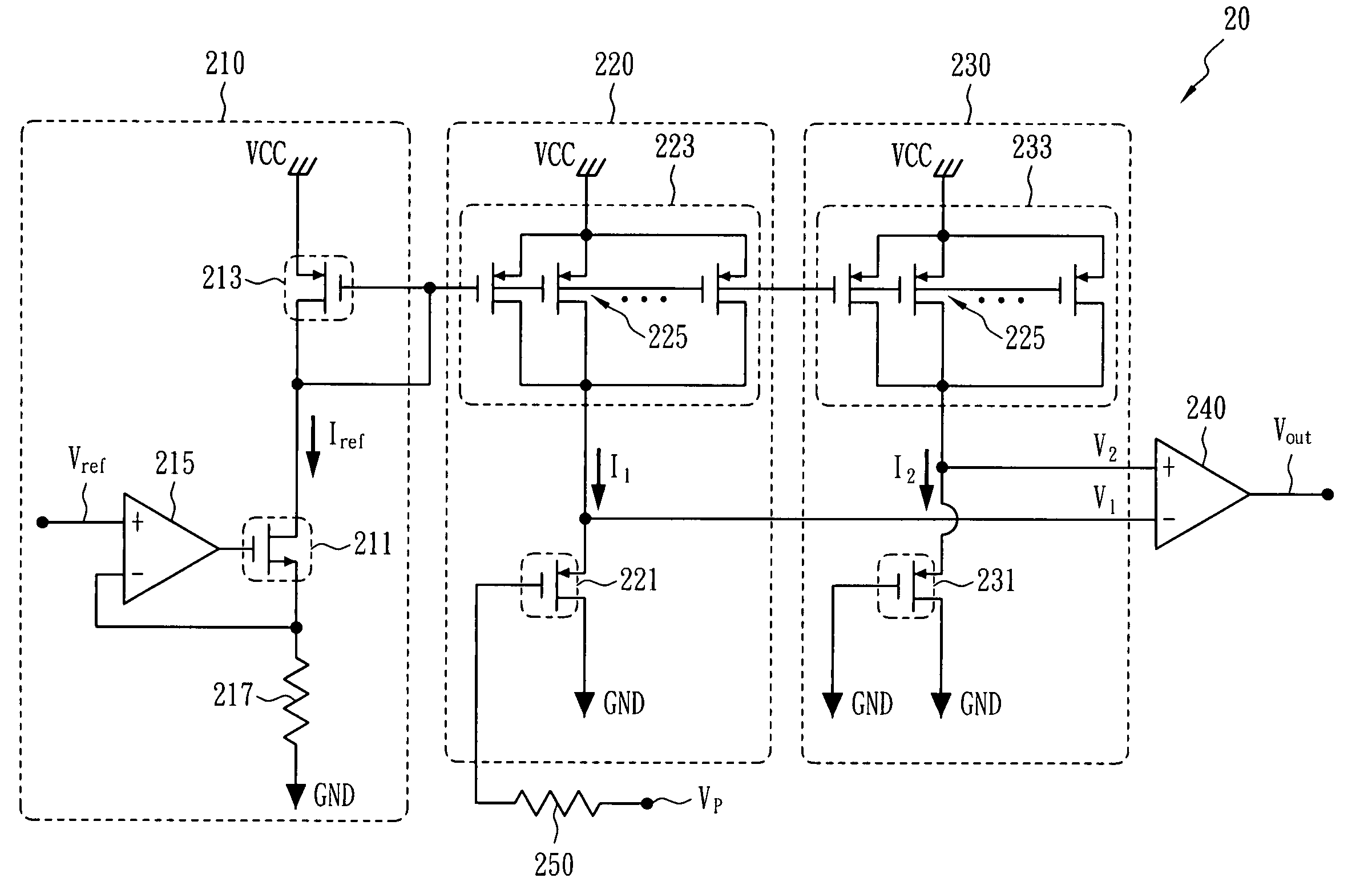
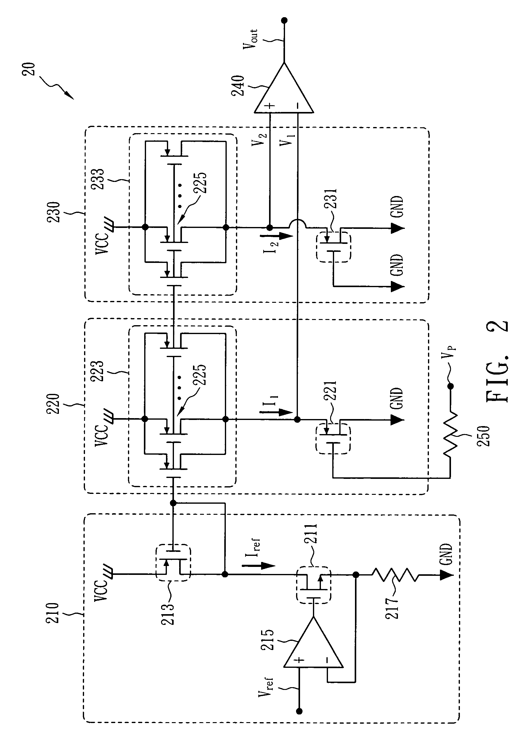
[0018]FIG. 2 shows a negative voltage detection circuit 20 for a synchronous rectifier MOSFET in accordance with an embodiment of the present invention. The negative voltage detection circuit 20 comprises a reference current source 210, a first circuit 220, a second circuit 230, and a comparator 240. The reference current source 210, the first circuit 220, and the second circuit 230 form a current mirror structure, wherein the transistors are FETs.

[0019]The reference current source 210 comprises a first transistor 211 (an NMOS type operational transistor), a second transistor 213 (a PMOS type load transistor), an operational amplifier 215, and a resistor 217. The first transistor 211, the second transistor 213, and the resistor 217 are connected in series. The input voltage at the positive input end of the operational amplifier 215 is a bandgap type reference voltage Vref which does not change along with the external environmental temperature so that the reference current source 210...


PUM


Abstract

A negative voltage detection circuit for a synchronous rectifier metal oxide silicon field effect transistor (MOSFET). The circuit comprises a reference current source, a first circuit mirroring a first current based upon the reference current source and generating a first voltage based upon a detection voltage, a second circuit mirroring a second current based upon the reference current source and generating a second voltage, and a comparator having input ends to receive the first voltage and the second voltage, wherein a level of an output voltage of the comparator changes when the detection voltage is equivalent to a value predetermined according to a difference between the first current and the second current.

Description

BACKGROUND OF THE INVENTION[0001]1. Field of the Invention[0002]The present invention relates to a negative voltage detection circuit, and more particularly to a negative voltage detection circuit for a synchronous rectifier MOSFET.[0003]2. Description of the Related Art[0004]FIG. 1 shows a conventional synchronous rectifier MOSFET circuit 10. A synchronous control circuit 100 is electrically connected to a gate 120b of a power transistor 120, so as to switch on or switch off the power transistor 120 by using an output control signal A. A parasitic body diode 121 exists between the drain 120a and the source 120c of the power transistor 120. The power transistor 120 has the advantages of a fast switching speed and a low turn-on resistance between the drain 120a and the source 120c, thus reducing the power consumption when the power transistor 120 is turned on.[0005]During a positive half-cycle of an AC input signal D, an input synchronous signal C of the synchronous control circuit 1...

Claims


Application Information

Patent Timeline
Patent Type & Authority Applications(United States)
IPC IPC(8): G01R19/22
CPCG01R19/16538H02M3/33592Y02B70/1475Y02B70/10
Inventor CHU, HUNG SUNGLIANG, SHEN YAO
Owner HIMAX TECH LTD
Why Eureka
Try Eureka