Organic photosensitive optoelectronic devices with nonplanar porphyrins

a technology of optoelectronic devices and porphyrins, which is applied in the direction of organic semiconductor devices, organic chemistry, nanoinformatics, etc., can solve the problems of energy loss, limiting the thickness of the organic layer to be used, and unsuitable resistive pathways for separated charges

Active Publication Date: 2008-12-18
UNIV OF SOUTHERN CALIFORNIA
View PDF5 Cites 31 Cited by
  • Summary
  • Abstract
  • Description
  • Claims
  • Application Information

AI Technical Summary

Problems solved by technology

However, the photocurrent is highly dependent on the charge transport properties of the materials, since resistivity to charge flow represents a significant challenge to cell performance2.
The exciton diffusion length is generally short for organic semiconductors relative to the optical absorption length LA, hence limiting the thickness of the organic layer to be used due to the relatively low ability of the excitons to reach the Donor-Acceptor interface for charge separation.
This effect not only restrains the amount of absorbing material but also creates a resistive pathway for separated charge that is undesirable for efficient light conversion1.
Yet, it is clear that the VOC does not reflect the total energy of the photons absorbed and that energy must be lost during the power conversion process.

Method used


Image

  • Organic photosensitive optoelectronic devices with nonplanar porphyrins
  • Organic photosensitive optoelectronic devices with nonplanar porphyrins
  • Organic photosensitive optoelectronic devices with nonplanar porphyrins

Examples


example

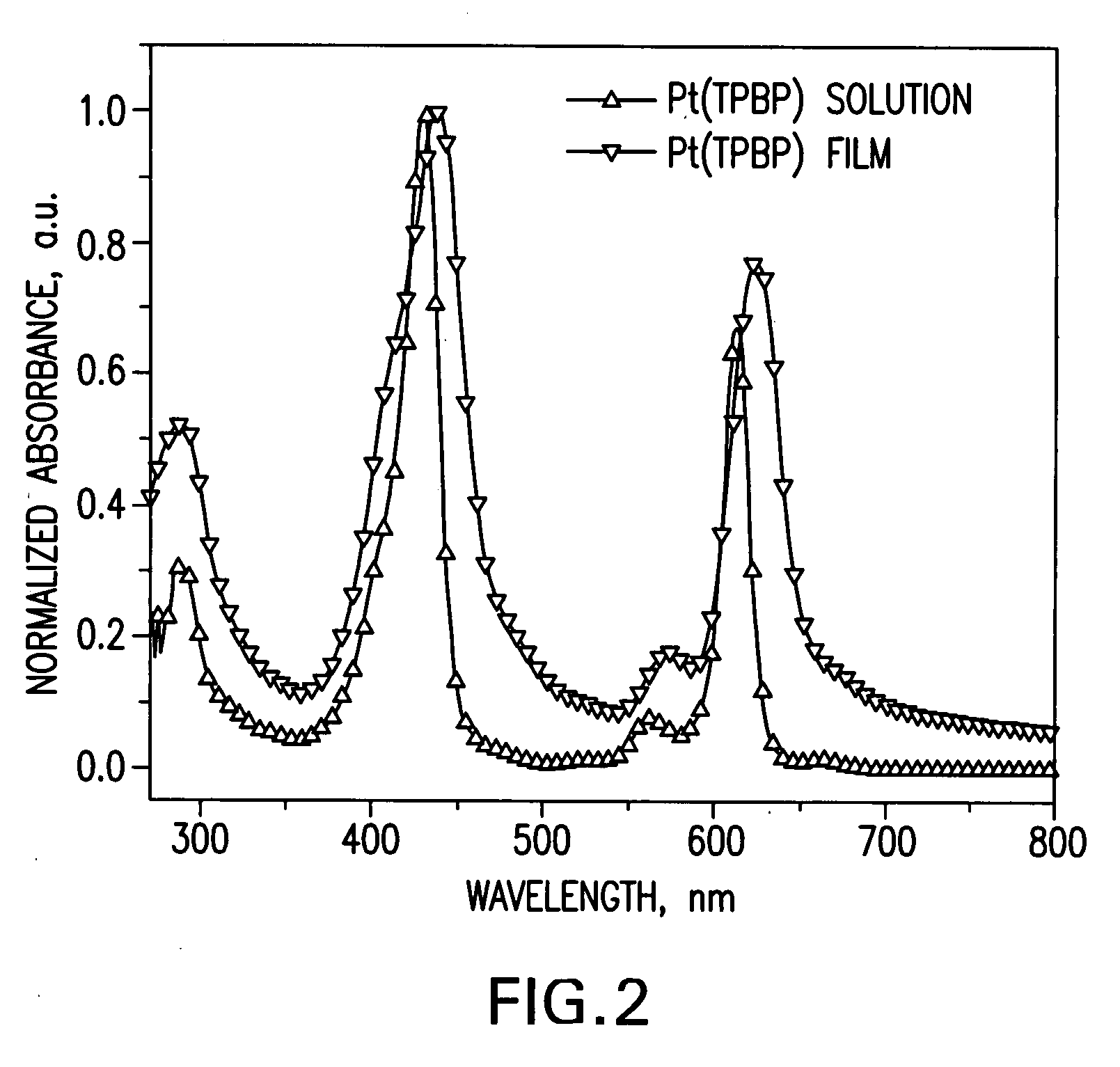
[0130]Photovoltaic cells were grown on ITO-coated glass substrates that were solvent cleaned8 and treated in UV-ozone for 10 minutes immediately prior to loading into a high vacuum (Base pressure 2×10⁻⁶ Torr) chamber. The organic materials, M(TPBP) (synthesized in house), CuPc (Aldrich), C60 (MTR Limited), and 2,9-dimethyl-4,7-diphenyl-1,10-phenanthroline (BCP) (Aldrich) were purified by sublimation prior to use. Metal cathode materials, Ag and Al (Alfa Aesar) were used as received. Materials were sequentially grown by vacuum thermal evaporation at the following rates: M(TPBP) (1 Å / sec), C60 (2 Å / sec), and 2,9-dimethyl-4,7-diphenyl-1,10-phenanthroline (BCP) (2 Å / sec) and metals: 1000 Å thick Ag (4 Å / sec) or Al (2.5 Å / sec). The cathode was evaporated through a shadow mask with 1 mm diameter openings. For solution processed donor, the layers where spin coated for 40 s at 3000 rpm for a final 100 Å and at 1500 rpm for 150 Å. The substrates where then annealed at 90° C. for 30 mins unde...


PUM

PropertyMeasurementUnit
valenceaaaaaaaaaa
valence atomaaaaaaaaaa
organicaaaaaaaaaa

Abstract

Embodiments of the present invention provide an organic photosensitive optoelectronic device comprising at least one nonplanar porphyrin of formula (I),wherein the meanings of M, R and R′ are disclosed herein.

Description

JOINT RESEARCH AGREEMENT[0001]The claimed invention was made by, on behalf of, and / or in connection with the following parties to a joint university-corporation research agreement: The University of Southern California and Global Photonic Energy Corporation. The agreement was in effect on and before the date the claimed invention was made, and the claimed invention was made as a result of activities undertaken within the scope of the agreement.FIELD OF THE INVENTION [0002]The present invention generally relates to organic photosensitive optoelectronic devices. More specifically, it is directed to organic photosensitive optoelectronic devices comprising at least one nonplanar porphyrin.BACKGROUND [0003]Optoelectronic devices rely on the optical and electronic properties of materials to either produce or detect electromagnetic radiation electronically or to generate electricity from ambient electromagnetic radiation.[0004]Photosensitive optoelectronic devices convert electromagnetic r...

Claims


Application Information

Patent Timeline
Patent Type & Authority Applications(United States)
IPC IPC(8): B05D1/36C09B47/04
CPCB82Y10/00C07D487/22H01L51/0046Y02E10/549H01L51/424H01L2251/308H01L51/0077H10K85/211H10K85/30H10K30/20H10K2102/103
Inventor THOMPSON, MARK E.PEREZ, MARIA DOLORESBOREK, CARSTEN
Owner UNIV OF SOUTHERN CALIFORNIA
Why Eureka
Try Eureka