Integrated Circuit Comprising an Organic Semiconductor, and Method for the Production of an Integrated Circuit

a technology of organic semiconductors and integrated circuits, applied in the direction of plastic/resin/waxes insulators, instruments, originals for photomechanical treatment, etc., can solve the problems of high process cost, low throughput, and high temperature of inorganic nitrides, and achieve the effect of high process cost and low cos

Inactive Publication Date: 2008-12-25
POLARIS INNOVATIONS LTD
View PDF30 Cites 4 Cited by
  • Summary
  • Abstract
  • Description
  • Claims
  • Application Information

AI Technical Summary

Benefits of technology

[0014]In one aspect, the present invention provides an integrated circuit comprising an organic semiconductor and a method in which the production of dielectric layers of an OFET is possible at low temperatures.
[0026]For good processibility, it is preferred that the proportion of base polymer, crosslinking component and photo acid generator is a proportion between 5 and 20% by mass.

Problems solved by technology

However, the high process costs and the low throughput are disadvantageous here for mass-produced products.
Similarly to the preparation of inorganic oxides, the deposits of inorganic nitrides require high temperatures or high process costs.
However, this crosslinking is effected at temperatures of 200° C., which is problematic for the production of flexible substrates having a large area.

Method used


Image

  • Integrated Circuit Comprising an Organic Semiconductor, and Method for the Production of an Integrated Circuit
  • Integrated Circuit Comprising an Organic Semiconductor, and Method for the Production of an Integrated Circuit
  • Integrated Circuit Comprising an Organic Semiconductor, and Method for the Production of an Integrated Circuit

Examples


Embodiment Construction

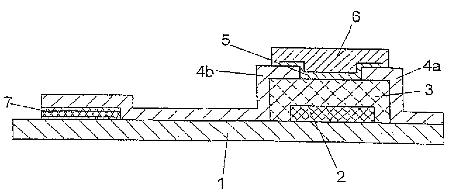
[0038]FIG. 1 shows the fundamental structure of such a transistor in a bottom contact architecture.

[0039]A gate electrode 2, which is covered by a gate dielectric layer 3, is arranged on a substrate 1. As will be explained later, in an embodiment of the process according to the invention the substrate 1 with the gate electrode 2 already arranged thereon constitutes the starting material on which the gate dielectric layer 3 is applied. A drain layer 4a and a source layer 4b, both of which are connected to the active semiconducting layer 5, are arranged on the gate dielectric layer 3. A passivating layer 6 is arranged above the active layer 5.

[0040]The source layer 4b produces a connection to the interconnect layer 7.

[0041]The deposition and processing of the gate dielectric layer 3 are preferred for that embodiment of the invention described here.

[0042]The circuits according to the invention and the production thereof solve the problem of the provision of OFETs having gate dielectric...


PUM

PropertyMeasurementUnit
temperatureaaaaaaaaaa
temperaturesaaaaaaaaaa

Abstract

An embodiment of the invention provides an integrated circuit having an organic field effect transistor (OFET) with a dielectric layer. The dielectric layer is prepared from a polymer formulation comprising: about 100 parts of at least one crosslinkable base polymer, from about 10 to about 20 parts of at least one di- or tribenzyl alcohol compound as an electrophilic crosslinking component, from about 0.2 to about 10 parts of at least one photo acid generator, and at least one solvent. Another embodiment provides a semiconductor fabrication method. The method comprises applying the polymer formulation to a surface of a substrate, drying the polymer formulation, crosslinking the polymer formulation after drying, and baking the polymer formulation after crosslinking.

Description

[0001]This application is a divisional of U.S. Ser. No. 11 / 362,960 filed on Feb. 27, 2006, which application is a continuation of International Application No. PCT / DE2004 / 001903, filed Aug. 24, 2004, which designated the United States and was not published in English, and which is based on German Application No. 103 40 608.5 filed Aug. 29, 2003, of which all applications are incorporated herein by reference.TECHNICAL FIELD[0002]The invention relates generally to integrated circuit manufacturing and more particularly to organic field effect transistors (OFET).BACKGROUND[0003]Systems comprising integrated circuits based on organic semiconductors, in particular organic field effect transistors (OFET), constitute a promising technology in the mass application sector of economical electronics. A field effect transistor is considered to be organic particularly if the semiconducting layer is produced from an organic material.[0004]Since it is possible to build up complex circuits using OFE...

Claims


Application Information

Patent Timeline
Patent Type & Authority Applications(United States)
IPC IPC(8): H01L51/05G03F1/90H01B3/18H01B3/44
CPCH01B3/442H01L51/052H10K10/471
Inventor HALIK, MARCUSKLAUK, HAGENSCHMID, GUENTERWALTER, ANDREASZSCHIESCHANG, UTE
Owner POLARIS INNOVATIONS LTD
Why Eureka
Try Eureka