Multiplication device comprising resin-dispersed organic semiconductor film and method for producing the same

a technology of organic semiconductor film and multiplication device, which is applied in thermoelectric devices, sustainable manufacturing/processing, and final product manufacturing, etc., can solve the problems of difficult to increase the area, increase the probability of conduction between the upper and lower electrodes, etc., and achieve the effect of easy production

Inactive Publication Date: 2005-04-12
JAPAN SCI & TECH CORP
View PDF9 Cites 4 Cited by
  • Summary
  • Abstract
  • Description
  • Claims
  • Application Information

AI Technical Summary

Benefits of technology

According to the present invention, a photocurrent multiplication device and a light-light conversion device are produced comprising a film made by coating the...

Problems solved by technology

Pinholes tend to be generated due to non-uniformity of the film, and this increases the probability of occu...

Method used


Image

  • Multiplication device comprising resin-dispersed organic semiconductor film and method for producing the same
  • Multiplication device comprising resin-dispersed organic semiconductor film and method for producing the same
  • Multiplication device comprising resin-dispersed organic semiconductor film and method for producing the same

Examples


first embodiment

(First Embodiment)

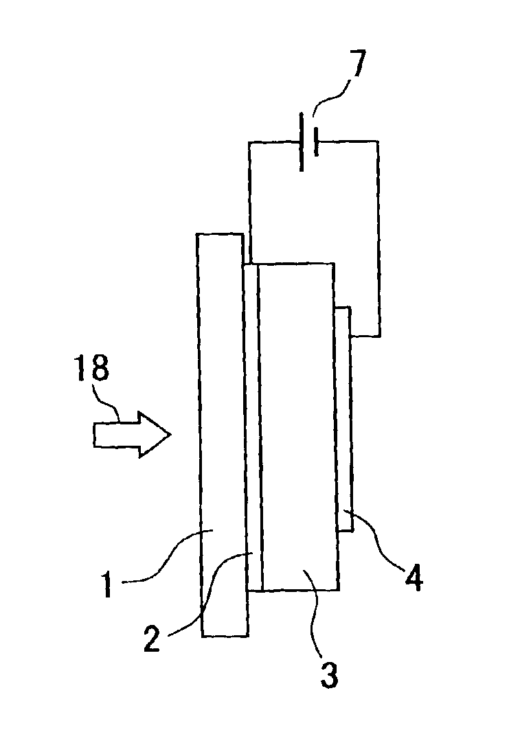
FIG. 5 shows an embodiment of the photocurrent multiplication device of the present invention schematically illustrated in FIG. 1 applied as a laboratory model. The electrode 2 serves as the lower electrode formed on the glass substrate 1 for applying a voltage to the resin-dispersed organic semiconductor layer 3. An ITO transparent electrode (thickness: about 0.05 μm) was used as the lower electrode 2. The resin-dispersed organic semiconductor layer 3 in which a photoconductive organic semiconductor is dispersed in a resin is formed on the glass substrate 1 covering the lower electrode 2. The electrode 4 serves as the upper electrode formed on the resin-dispersed organic semiconductor layer 3, and is made of a gold evaporated film having a thickness of about 0.02 μm. The upper electrode 4 is composed of a plurality of pieces placed apart from one another so as to enable measurement of the photocurrent at different places because this embodiment is a laboratory mod...

second embodiment

(Second Embodiment)

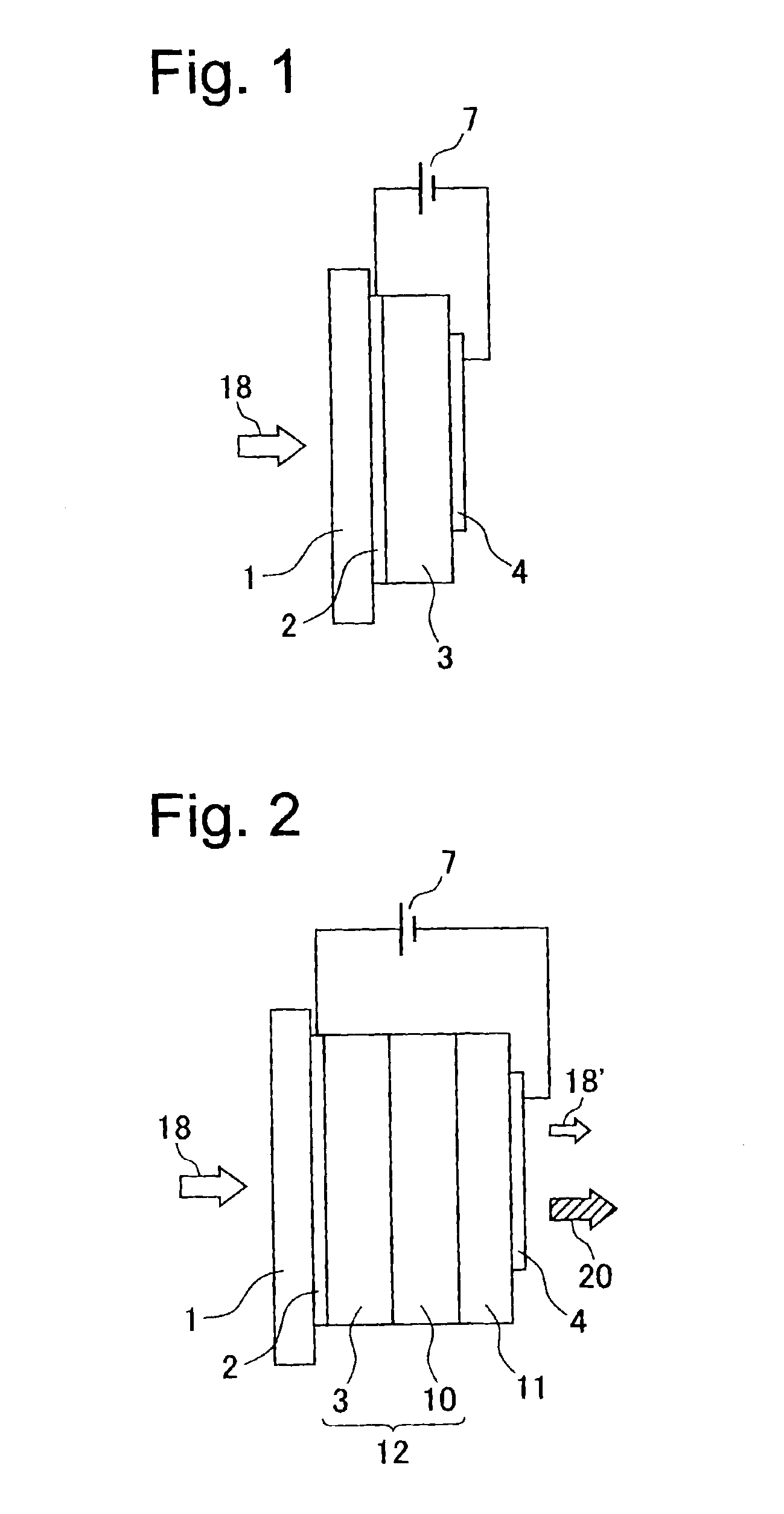
In Second Embodiment, the present invention is applied to a light-light conversion device, of which construction is shown in FIG. 2.

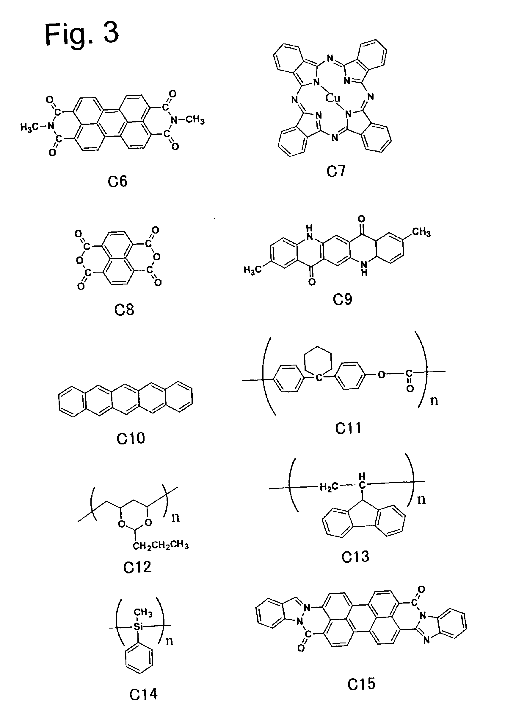
The lower electrode 2 is an ITO transparent electrode formed on the glass substrate 1. The resin-dispersed organic semiconductor layer 3 as the photocurrent multiplication layer is made of Im-perylene pigment dispersed in polycarbonate at a dispersion concentration of 50%. The thickness of the layer is 0.5 μm. As the organic electroluminescent layer 10 formed integrally on the resin-dispersed organic semiconductor layer 3, used was an evaporated film of an aluminum-quinolinol complex (Alq3) shown as chemical formula C12 in FIG. 4. As the hole transport layer 11 provided between the resin-dispersed organic semiconductor layer 3 and the upper electrode 4, used was an evaporated film of a triphenyl-diamine derivative (TPD) shown as chemical formula C13 in FIG. 4. As the upper electrode 4, a gold evaporated film was used.

FIG. 9 shows the ...


PUM

PropertyMeasurementUnit
Electrical conductoraaaaaaaaaa
Electric potential / voltageaaaaaaaaaa
Photoconductivityaaaaaaaaaa

Abstract

A resin-dispersed organic semiconductor layer (3) is formed on a lower electrode (2) of an ITO transparent electrode formed on a glass substrate (1). An upper electrode (4) of a gold deposited film is formed on the resin-dispersed organic semiconductor layer (3). The resin-dispersed organic semiconductor layer (3) is formed by spin-coating a dispersion liquid prepared by mixing a perylene pigment and polycarbonate in a THF solvent and drying the coating. By applying a voltage by means of the electrodes (2, 4) and by irradiating the resin-dispersed organic semiconductor layer (3) with light, a multiplied light irradiation-induced current flows.

Description

BACKGROUND OF THE INVENTION1. Field of the InventionThe present invention relates to organic optoelectronic devices, and more particularly, relates to a photocurrent multiplication device comprising a photocurrent multiplication phenomenon brought about by a photoconductive organic semiconductor and a light-light conversion device additionally including an organic electroluminescent layer for obtaining light-light converted light, and relates to methods for producing such devices.2. Background ArtIn the past, a photocurrent multiplication phenomenon exhibiting a photocurrent quantum yield exceeding ten thousand has been reported to occur in a device including a vacuum-evaporated film made of an organic pigment as a photocurrent multiplication layer and two metal electrodes sandwiching the photocurrent multiplication layer (see M. Hiramoto, T. Imahigashi and M. Yokoyama, Appl. Phys. Lett., 64, 187 (1994)).However, such a photocurrent multiplication phenomenon occurring in an organic ...

Claims


Application Information

Patent Timeline
IPC IPC(8): C09K11/06H01L21/70H01L31/14H01L21/8238H01L31/09H01L31/08H01L51/00H05B33/14H05B33/10H05B33/22H05B33/12H01L51/05H01L51/50
CPCH01L31/141H01L51/4206H01L51/0035H01L51/004H01L51/0052Y02E10/549H01L51/0081H01L2251/308H01L51/0053Y02P70/50H10K85/111H10K85/141H10K85/621H10K85/615H10K85/324H10K30/451H10K2102/103
Inventor YOKOYAMA, MASAAKINAKAYAMA, KEN-ICHIHIRAMOTO, MASAHIRO
Owner JAPAN SCI & TECH CORP
Why Eureka
Try Eureka