
Diode Structure

a diode and diode technology, applied in the field of backtoback diode structure, can solve the problems of increased capacitance, high current leakage and capacitance of zener diodes, and suffer from high conductivity modulated resistance, so as to minimise manufacturing tolerances in vpt

Inactive Publication Date: 2008-12-25
UNIV COLLEGE CORK NAT UNIV OF IRELAND CORK
View PDF5 Cites 3 Cited by
  • Summary
  • Abstract
  • Description
  • Claims
  • Application Information

AI Technical Summary

Benefits of technology

[0018]In one embodiment, the doping of the base is set to a level such that injected current level per unit area (Jcrit) at which the conductivity modulation occurs due to avalanche behaviour is increased.
[0019]In one embodiment, the device has a double-base structure, and the width of a lower-doped base region is minimised such that current density Jcrit at which the conductivity modulation occurs due to avalanche is increased.
[0023]In one embodiment, thickness of N− or P− layers is minimised such that the current-carrying capability is maximised and the doping of this layer does not affect the current-carrying capability of the device.
[0026]In one embodiment, the N− or P− layer doping is sufficiently low such that the N− or P− layer is fully depleted pre-breakdown and the capacitance of the device is minimised.
[0028]In one embodiment, the N− or P− layer is sufficiently wide such that, when biased for punchthrough breakdown, it is wider than the sum of the manufacturing tolerance of this layer and the depletion region formed in this layer due to the applied bias so that the manufacturing tolerances in Vpt are minimised.

Problems solved by technology

However, at low voltages, the leakage current and capacitance of a Zener diode is too high for many mobile and high frequency applications.
The band-to-band tunneling mechanism requires much higher doping levels which result in the increased capacitance.
The punchthrough diode exhibits low leakage characteristics but suffers from high conductivity modulated resistance at high current levels.
Such open base bipolar diodes exhibit low leakage also, but suffer from a large negative resistance region at low current levels which may induce significant instability in the device.
This is described as disadvantageous due to instabilities, and the approach was to design such that this negative differential resistance and associated avalanche breakdown did not occur.

Method used


Image

  • Diode Structure
  • Diode Structure
  • Diode Structure

Examples


Embodiment Construction

[0032]The invention will be more clearly understood from the following description of some embodiments thereof, given by way of example only with reference to the accompanying drawings in which:—

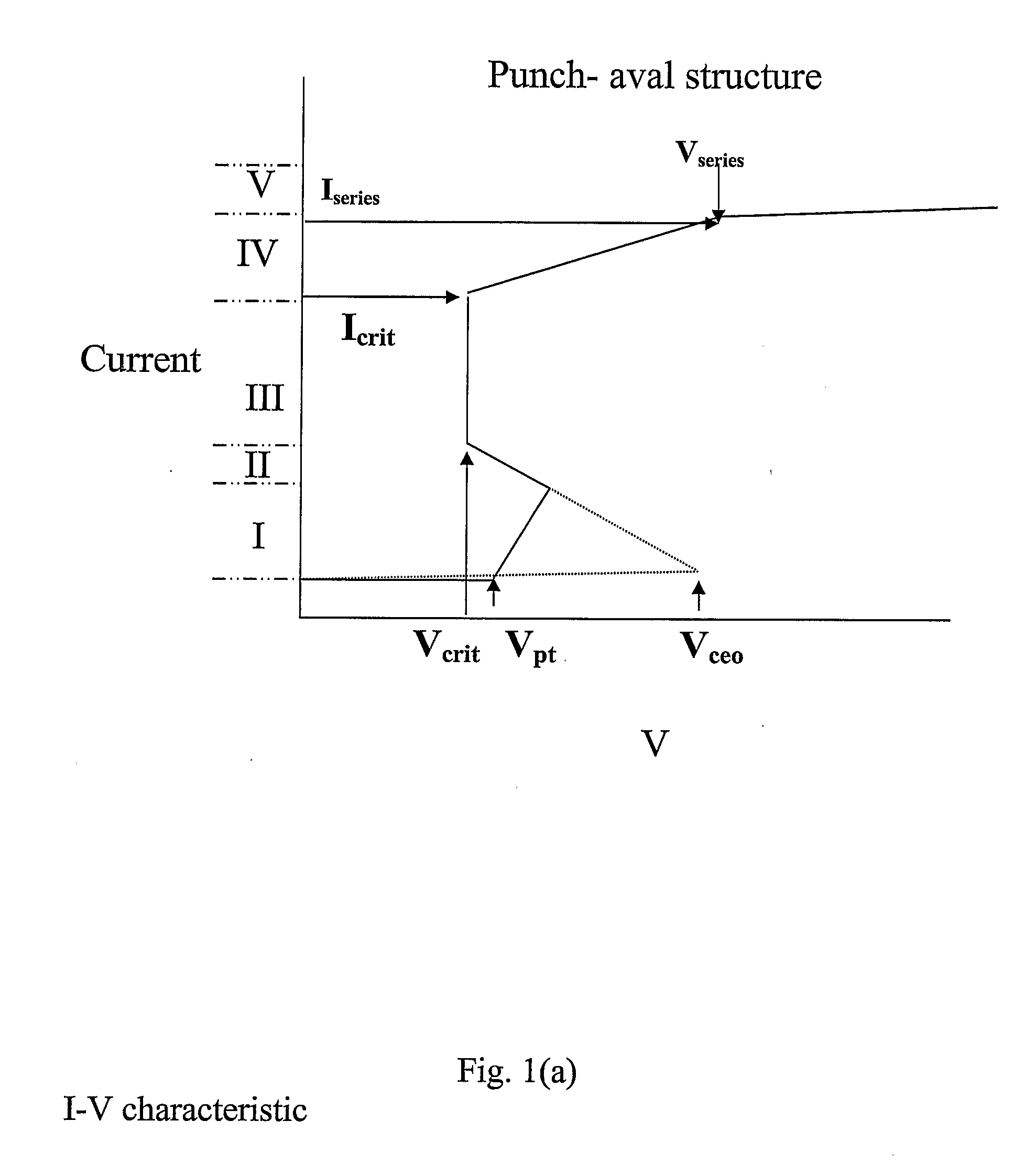
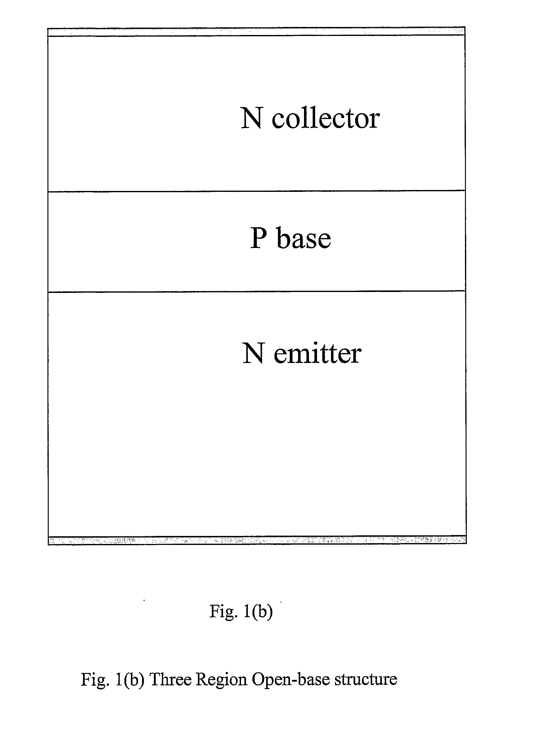
[0033]FIG. 1(a) is a diagrammatic representation of the I-V characteristic at breakdown of a three region open base structure of the invention, shown in FIG. 1(b);

[0034]FIGS. 2 to 11 are simulated and measured plots demonstrating performance;

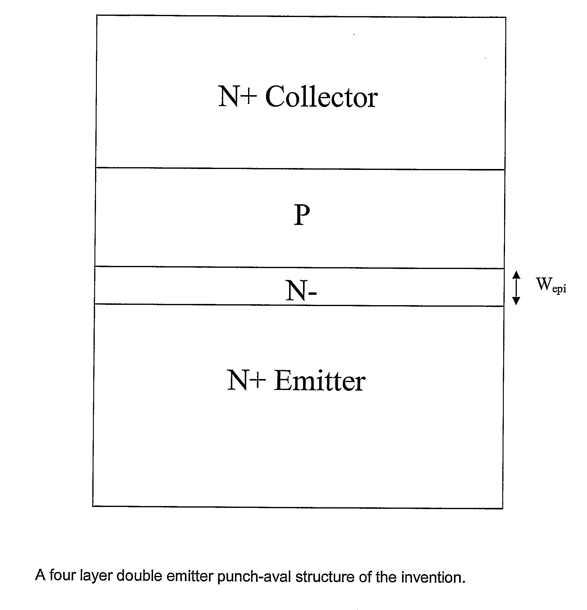
[0035]FIG. 12 is a diagram of a four-layer structure of the invention termed a double-emitter structure;

[0036]FIGS. 13 to 15 are simulated plots demonstrating performance of the four-layer structure; and

[0037]FIG. 16 is a diagram of a bidirectional five-layer structure.

[0038]This invention provides a hybrid punchthrough-avalanche device which exhibits low leakage punchthrough breakdown at low current levels followed by avalanche breakdown at higher current levels. In particular, the behaviour of this structure after conductivity modulation occurs is exam...


PUM


Abstract

An open-base semiconductor diode device has an emitter, base, and collector layers. The layers are configured and doped such that the device has an IV characteristic with: i. a punchthrough region beginning at a voltage Vpt with positive resistance, followed by, and ii. an avalanche region including a positive resistance stage beginning with conductivity modulation at Vcrit and Icrit and having a resistance Rcrit, iii. wherein the values of Vcrit, Icrit and Rcrit are set according to the layer configuration and doping. The device may have a double-base structure, and the width of a lower-doped base region may be minimised such that current density Jcrit at which the conductivity modulation occurs due to avalanche is increased. In one example, the device comprises a N-N+ or a P-P+ double-emitter. Thickness of N− or P− layers may be minimised such that the current-carrying capability is maximised and the doping of this layer does not affect the current-carrying capability of the device.

Description

FIELD OF THE INVENTION[0001]The invention relates to a back-to-back diode structure, also termed an open base structure and to the manner in which it is designed and operated. This structure has electrical contact to the top and bottom regions but the middle region is not contacted. It relates particularly, but not exclusively, to clamping diodes for voltage and current suppression.PRIOR ART DISCUSSION[0002]The Zener diode is the most commonly used discrete semiconductor device for overvoltage and overcurrent protection of solid state circuits. However, at low voltages, the leakage current and capacitance of a Zener diode is too high for many mobile and high frequency applications. The reason for this higher current and capacitance is due to the breakdown mechanism changing from avalanche to band-to-band tunneling for low voltages (<4V). The band-to-band tunneling mechanism requires much higher doping levels which result in the increased capacitance. The increase in leakage curre...

Claims


Application Information

Patent Timeline
Patent Type & Authority Applications(United States)
IPC IPC(8): H01L29/70H01L21/329
CPCH01L29/8618
Inventor DUANE, RUSSELL
Owner UNIV COLLEGE CORK NAT UNIV OF IRELAND CORK
Learn More