

Semiconductor device having a dual gate electrode and methods of making the same
- Summary
- Abstract
- Description
- Claims
- Application Information
AI Technical Summary
Benefits of technology
Problems solved by technology
Method used
Image

Examples
Embodiment Construction
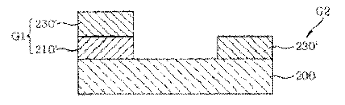
[0028]In general, example embodiments of the invention relate to semiconductor devices having a dual gate electrode, as well as methods for forming a dual gate electrode of a semiconductor device. Disclosed embodiments provide a number of advantages over the prior art, including but not limited to improvements in manufacturing productivity by reducing masking steps, and improvement in performance by making gate electrodes of PMOS and NMOS regions have a different thickness and material state.
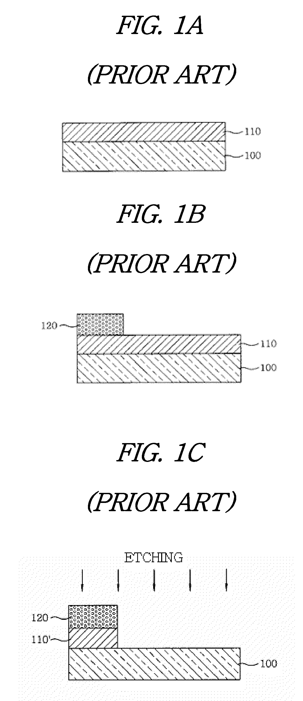
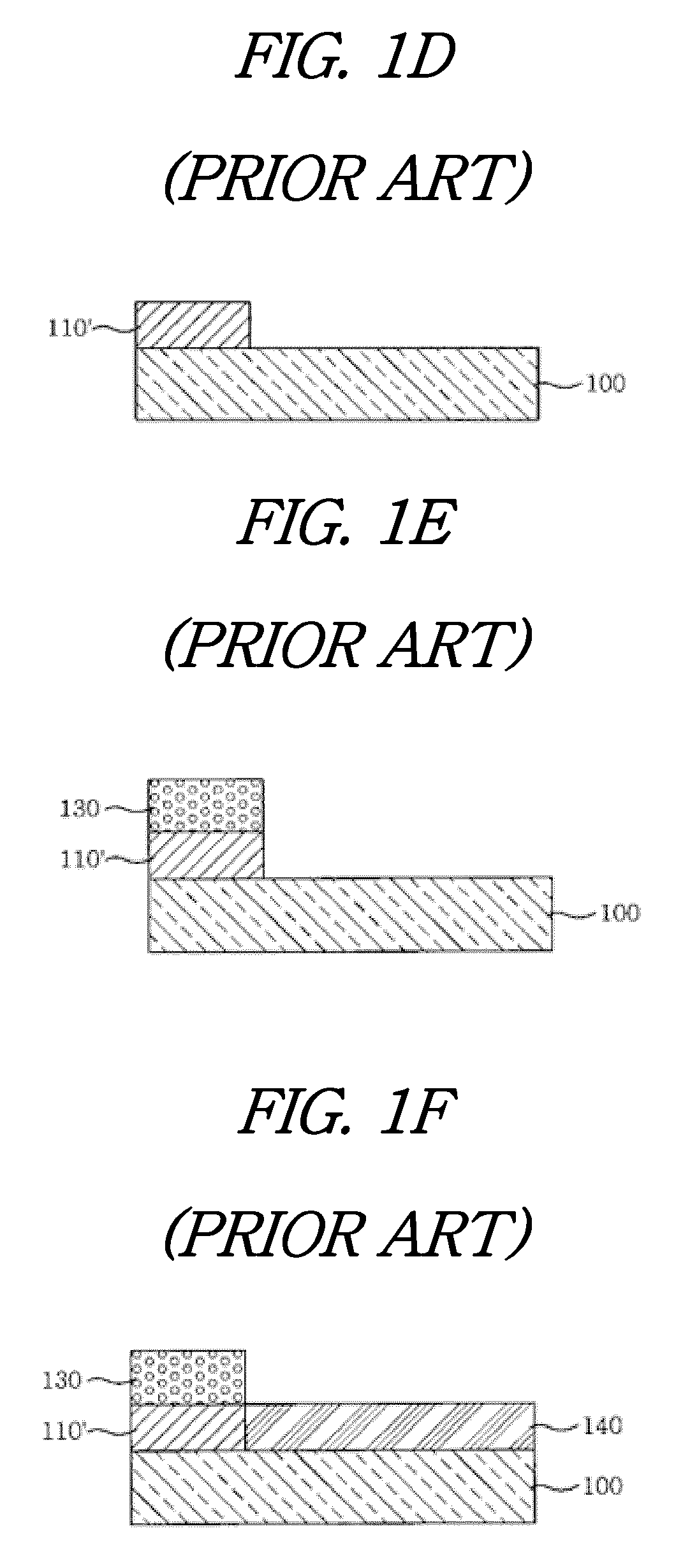
[0029]In accordance with an example embodiment, there is provided a method for forming a dual gate electrode of a semiconductor device, comprising the steps of: forming a first polysilicon layer over the entire surface of a semiconductor substrate; forming a first photoresist pattern on the first polysilicon layer so as to close a first region, the first region being one of a PMOS and an NMOS region; leaving the first polysilicon layer only in the first region by removing an exposed portion of t...
PUM
 Abstract
Description
Claims
Application Information