Imaging device and apparatus installed with the same

a technology of authentication apparatus and imaging device, which is applied in the field of imaging device for authentication apparatus, can solve the problems of deteriorating display image quality, inability to increase detection sensitivity, and inability to fully detect light reflected from objects, so as to reduce the circuit size, and widen the imaging and radiation conditions

Inactive Publication Date: 2008-12-25
HITACHI LTD
View PDF4 Cites 50 Cited by
  • Summary
  • Abstract
  • Description
  • Claims
  • Application Information

AI Technical Summary

Benefits of technology

[0030]wherein the light source control means causes the imaging light source units and the display light source units to radiate light during the accumulation time. This structure and the control operation makes it possible to display and pick up an image at the same time. Further, since the imaging circuit and the display circuit are not required to be operated in synchronism with each other, the control operation at a different rate is made possible and the imaging and radiation conditions are widened. Furthermore, the need of the synchronizing circuit is eliminated and the circuit size reduced.
[0031]Ac

Problems solved by technology

In the structure described in JP-A-2005-242841 and JP-A-2005-276030, however, the detection element array is required to transmit the light, and therefore, cannot be increased in detection sensitivity, thereby posing the problem that the light reflected from the object cannot be fully detected.
Also, the fact that the display and imaging light are attenuated poses the problem that the display image quality is deteriorated and the power is consumed for radiation of the light not used.
Further, the display and the imaging operation cannot be performed at the same time.
The structure described in JP-A-2006-86333, on the other hand, encounters the problem that the fill factor of the detection element array cannot be increased and the light reflected from the object cannot be sufficiently detected.
Also, since the display and imaging light is output through the detection elements, the problems are posed that the image displayed is dark, the display position resolution is deteriorated or otherwise the image quality is adversely affected, and the power is consumed for radiation of the unrequired light.
Further, the realization of a structure transmitting the light only through the detection elements increases the cos

Method used


Image

  • Imaging device and apparatus installed with the same
  • Imaging device and apparatus installed with the same
  • Imaging device and apparatus installed with the same

Examples


first embodiment

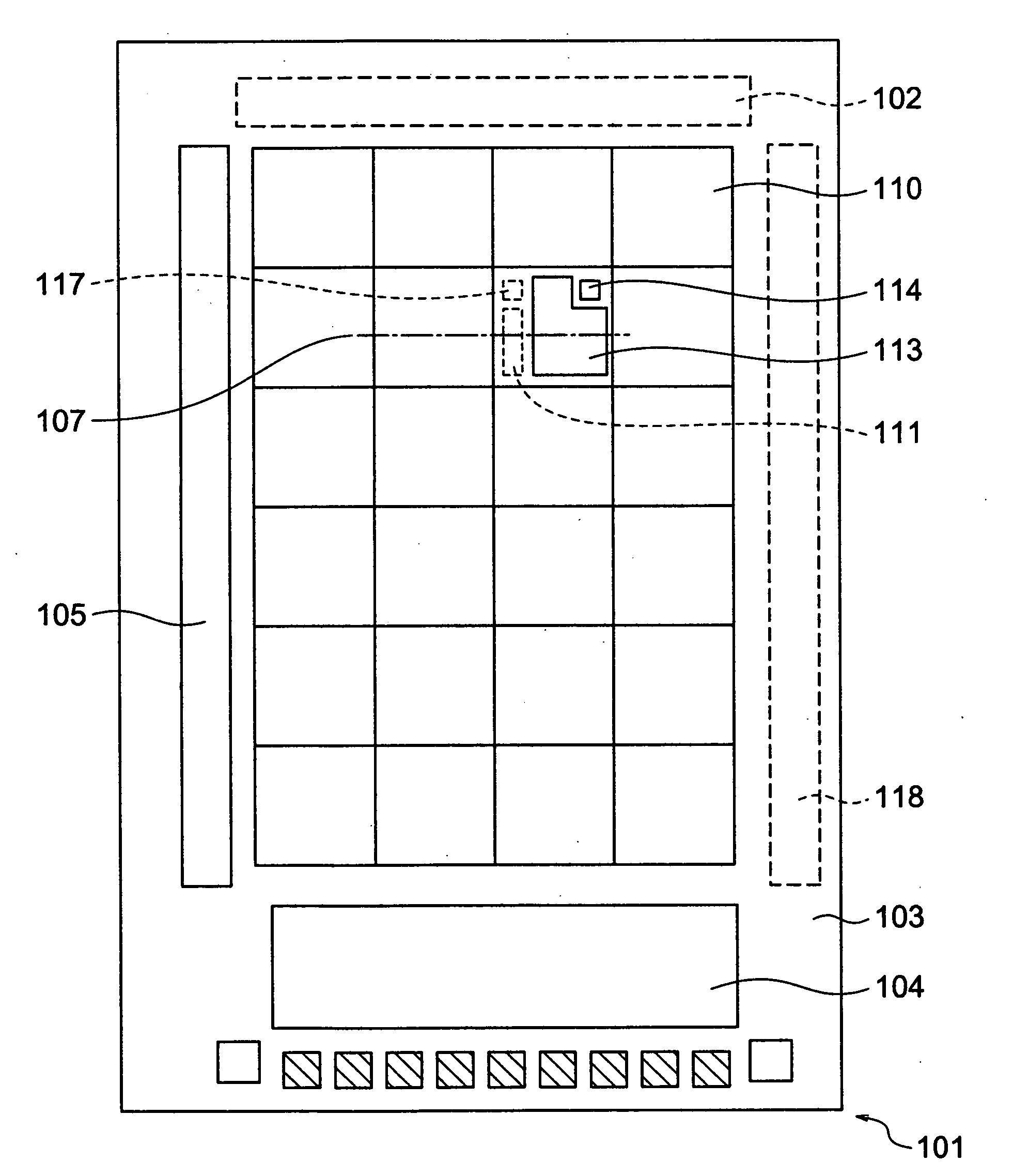
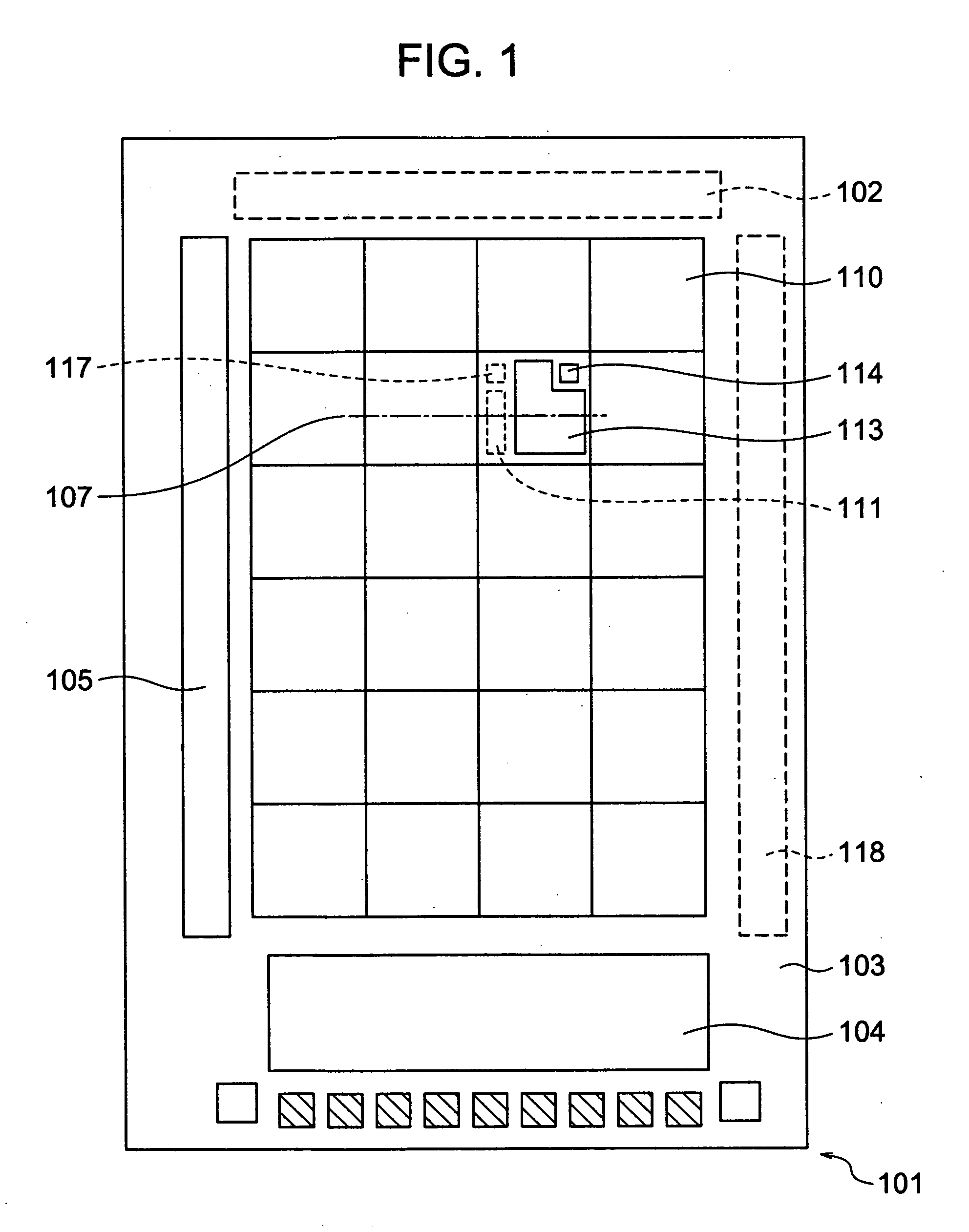
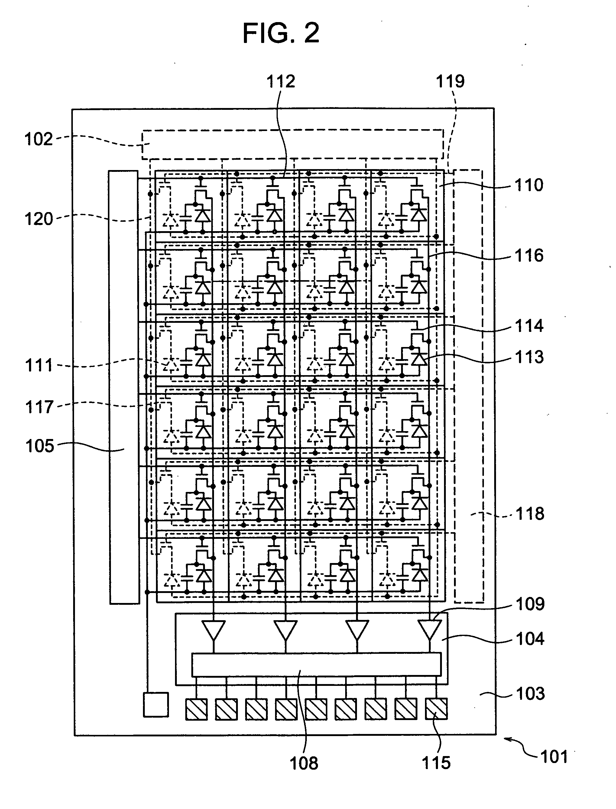
[0071]This embodiment represents an imaging device with an imaging light source as an application of the invention, and has a structure in which a light-emitting layer is arranged on a detection element layer. The first embodiment of the invention is explained below with reference to FIGS. 1 to 5. FIG. 1 is a view showing a general configuration of an example of the imaging device according to this embodiment, FIG. 2 a circuit diagram for explaining the circuit configuration of the imaging device 101, FIG. 3 a sectional view of the imaging device taken at position 107 in FIG. 1, FIG. 4 a diagram for explaining the conditions to block the incidence of the direct light from the light source units in FIG. 3, and FIGS. 5 to 7 diagrams for explaining the method of fabricating the imaging device 101.

[0072]With reference to FIG. 1, this embodiment is explained briefly. The imaging device 101 comprises a light source system (dotted line) for radiating the imaging light, and an optical senso...

second embodiment

[0104]The imaging device 101 according to this embodiment is different from the first embodiment in that a collimator layer is used as a means for preventing the entrance of the direct light into each detection element 113 from the light source units 111. FIG. 8 is a sectional view for explaining the structure of an example of the imaging device according to this embodiment taken at position 107 in FIG. 1. FIG. 9 is a diagram for explaining the conditions for preventing the entrance of the direct light from the light source units 111 in FIG. 8.

[0105]In the imaging device 101 according to this embodiment, a collimator layer 136 is formed between the light source unit layer 132 with the light source units 111 formed on the glass substrate 124 and the detection element layer 133 with the detection elements 113 formed on the glass substrate 125, which are bonded to each other by transparent package adhesives 131, 134. The collimator layer 136 has a structure in which light-blocking plat...

third embodiment

[0113]The imaging device 101 according to this embodiment is different from the second embodiment in the signal reading method. FIG. 10 is a diagram showing a general configuration of an example of the imaging device according to this embodiment. FIG. 11 is a sectional view of the imaging device. FIG. 12 is a timing chart for explaining the timing at which the light is radiated and the signal is read.

[0114]In the imaging device 101 according to this embodiment, as shown in FIG. 10, the pixels 110 each having the light source unit 111 and the detection element 113 are arranged two-dimensionally. A given pixel arranged in column x and row y is referred to as the pixel 110-x-y. The light source unit 111 and the detection element 113 are also designated similarly.

[0115]The imaging device 101 according to this embodiment, like the structure of the second embodiment, uses the collimator layer 136. As shown in FIG. 11, however, only one light-blocking plate 143 is arranged for each pixel s...


PUM


Abstract

An imaging device includes a light source layer having imaging light source units for radiating the imaging light containing a first wavelength on an object to be imaged, a detection layer having detection elements for detecting the light of the first wavelength radiated from the light source units, and a light-blocking unit interposed between the light source layer and the detection layer. The light source layer is held between the detection layer and the object to be imaged. The light-blocking unit is arranged in such a manner as to block the direct radiation of at least part of the light radiated from the light source units to the detection elements.

Description

INCORPORATION BY REFERENCE[0001]The present application claims priority from Japanese application JP2007-165766 filed on Jun. 25, 2007, the content of which is hereby incorporated by reference into this application.BACKGROUND OF THE INVENTION[0002]This invention relates to an imaging device for an authentication apparatus using the finger veins, the palm veins, the veins of the back of the hand or the fingerprint, and an imaging device for the portable terminal such as the mobile phone, the PDA or the PC or the image reader such as the facsimile or the scanner.[0003]A finger authentication apparatus is described below as a typical case.[0004]The password has been widely used in an authentication method for identifying an individual person. Now that a more accurate authentication technique is in demand, however, the biological authentication is closely watched. This authentication method, which uses the features of a part of a living creature or the motion thereof (biological informa...

Claims


Application Information

Patent Timeline
IPC IPC(8): G06K9/00G06V10/141A61B5/117G06T1/00H04N1/028H04N1/04H04N1/19H04N5/225H04N5/335H04N5/369
CPCG06K9/2027G06K2009/00932G06V40/14G06V10/141
Inventor KONNO, YASUTAKAUEKI, HIRONORI
Owner HITACHI LTD
Why Eureka
Try Eureka