Tft Substrate, Reflective Tft Substrate and Method for Manufacturing These Substrates

a technology of reflective tft and substrate, which is applied in the direction of transistors, optics, instruments, etc., can solve the problems of increasing manufacturing costs, reducing production yield, and complicated production processes, so as to reduce production steps, reduce production costs, and improve production efficiency

Inactive Publication Date: 2009-01-01
IDEMITSU KOSAN CO LTD
View PDF10 Cites 68 Cited by
  • Summary
  • Abstract
  • Description
  • Claims
  • Application Information

AI Technical Summary

Benefits of technology

[0073]Due to such a configuration, the number of masks used in the production can be decreased, leading to the reduction of production steps. As a result, production efficiency can be improved and manufacturing cost can be reduced.
[0074]Usually, the source wire, the drain wire, the source electrode, the drain electrode and the pixel electrode are formed from the reflective metal layer. By doing this, the source wire, the drain wire, the source electrode, the drain electrode and the pixel electrode can be produced efficiently.

Problems solved by technology

So many production steps may decrease production yield.
In addition, many steps may make the production process complicated and also increase the manufacturing cost.

Method used


Image

  • Tft Substrate, Reflective Tft Substrate and Method for Manufacturing These Substrates
  • Tft Substrate, Reflective Tft Substrate and Method for Manufacturing These Substrates
  • Tft Substrate, Reflective Tft Substrate and Method for Manufacturing These Substrates

Examples


first embodiment

[Method for Producing a TFT Substrate ]

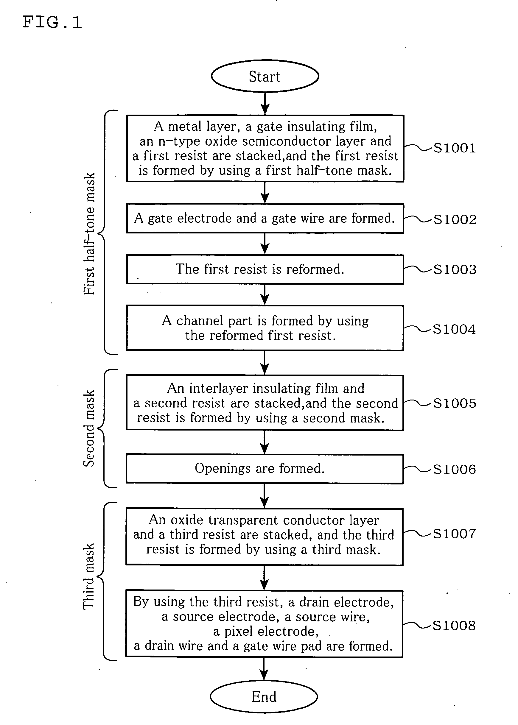
[0362]FIG. 1 is a schematic flow chart for explaining the method for producing a TFT substrate according to a first embodiment of the invention. The method for producing a TFT substrate in this embodiment corresponds to claim 24.

[0363]In FIG. 1, first, a metal layer 1020 as a thin film for a gate electrode / gate wire, a gate insulating film 1030, an n-type oxide semiconductor layer 1040 as a first oxide layer, and a first resist 1041 are stacked in this order on a glass substrate 1010, and the first resist 1041 is formed into a predetermined shape with a first half-tone mask 1042 by half-tone exposure (Step S1001).

[0364]Next, treatment using the first half-tone mask 1042 will be explained below referring to the drawing.

(Treatment Using a First Half-Tone Mask)

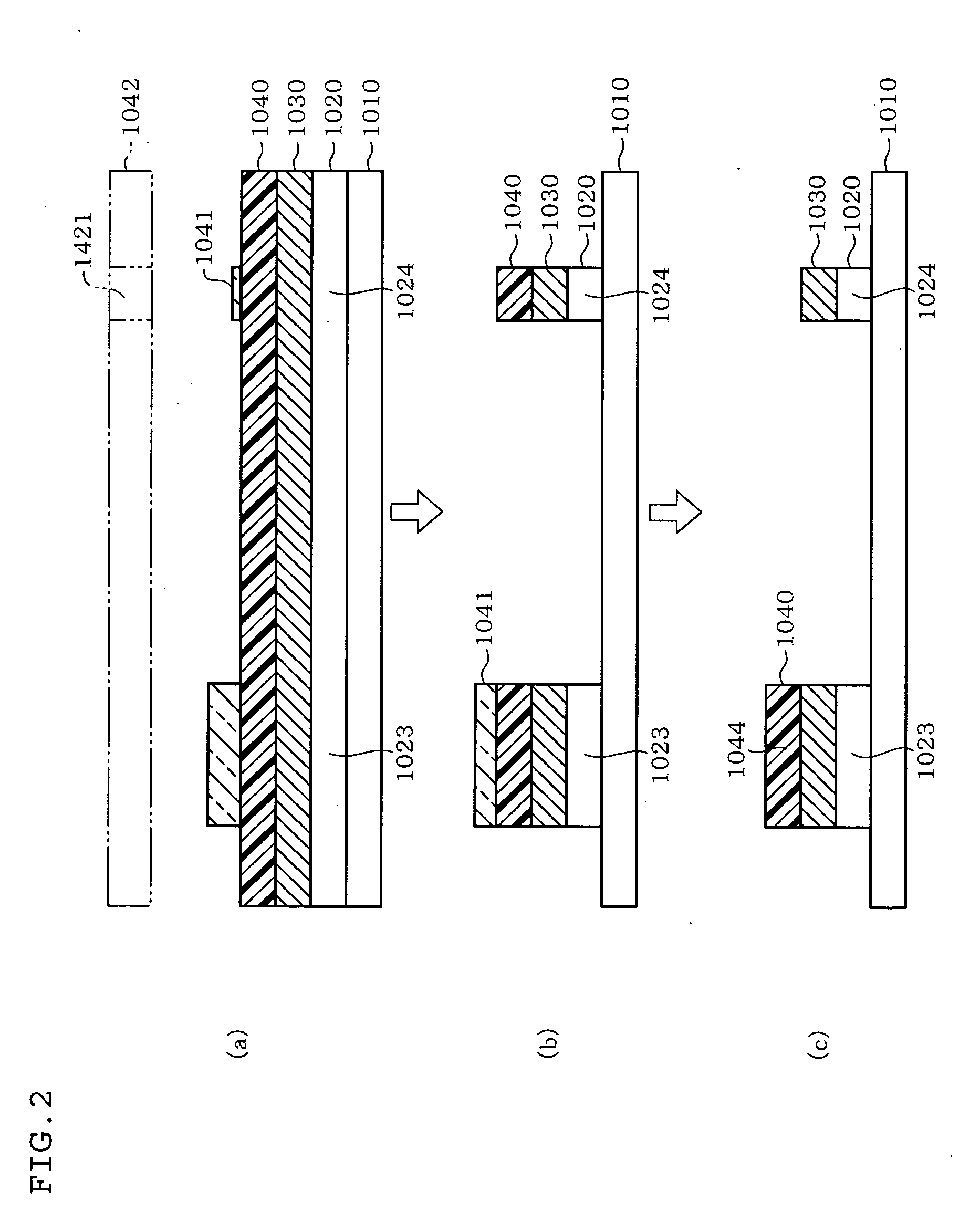
[0365]FIG. 2 is a schematic view for explaining treatment using a first half-tone mask in the method for producing a TFT substrate according to the first embodiment of the invention, in whic...

second embodiment

[Method for Producing a TFT Substrate ]

[0416]FIG. 8 is a schematic flow chart for explaining the method for producing a TFT substrate according to a second embodiment of the invention. The method for producing a TFT substrate in this embodiment corresponds to claim 25.

[0417]The method for producing the TFT substrate 1001a according to this embodiment shown in FIG. 8 differs from the above-mentioned method according to the first embodiment in the following points. Specifically, steps S1007 and S1008 of the first embodiment are changed as follows. That is, the oxide transparent conductor layer 1060, the protective insulating film 1070 and the third resist 1071 are stacked, and the third resist 1071 are formed by using a third half-tone mask 1072 (Step S1007a). Further, by using the third resist 1071, the drain electrode 1064, the source electrode 1063, the source wire 1065, the pixel electrode 1067, the drain wire 1066 and the gate wire pad 1025 are formed (Step S1008a). Then, the thi...

third embodiment

[Method for Producing a TFT Substrate ]

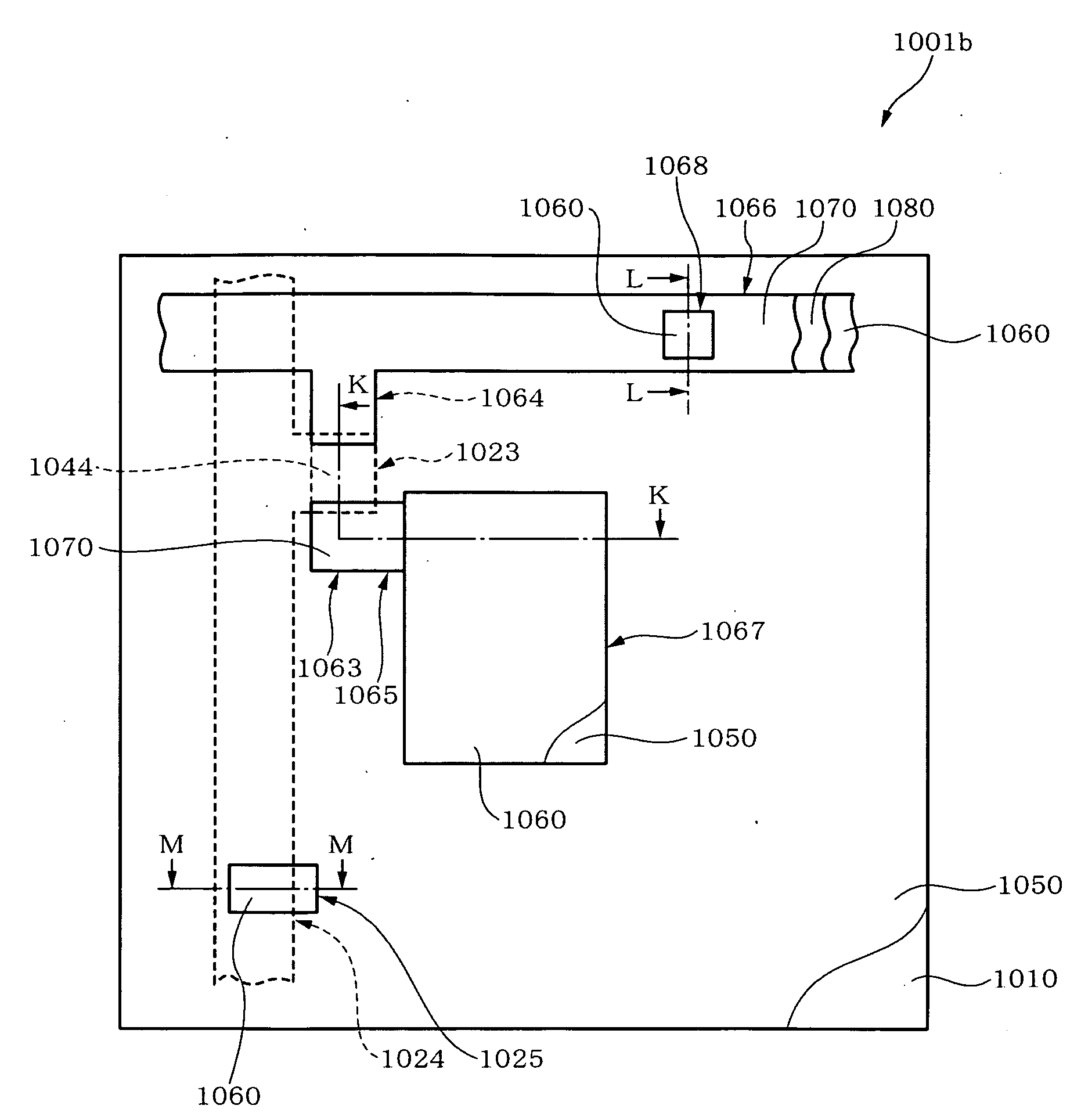
[0450]FIG. 16 is a schematic flow chart for explaining the method for producing a TFT substrate according to a third embodiment of the invention. The method for producing a TFT substrate in this embodiment corresponds to claim 27.

[0451]The method for producing the TFT substrate 1001b according to this embodiment shown in FIG. 16 differs from the above-mentioned method according to the second embodiment in the following point. Specifically, step S1007a of the second embodiment is changed as follows. That is, the oxide transparent conductor layer 1060, an auxiliary conductive layer 1080, the protective insulating film 1070 and the third resist 1071 are stacked, and the third resist 1071 is formed by using the third half-tone mask 1072 (Step S1007b). That is, the method shown in FIG. 16 differs from the above-mentioned second embodiment in this point.

[0452]Other steps are almost the same as those in the second embodiment. Therefore, in the drawing...


PUM


Abstract

An object of the invention is to propose a TFT substrate and a reflective TFT substrate which can be operated stably for a prolonged period of time, can be prevented from being suffering from crosstalk, and is capable of significantly reducing manufacturing cost by decreasing the number of production steps, as well as to propose the method for producing these substrates.
A TFT substrate 1001 comprises: a glass substrate 1010; a gate electrode 1023 and a gate wire 1024 insulated by having their top surfaces covered with a gate insulating film 1030 and by having their side surfaces covered with an interlayer insulating film 1050; an n-type oxide semiconductor layer 1040 formed on the gate insulating film 1030 above the gate electrode 1023; an oxide transparent conductor layer 1060 formed on the n-type oxide semiconductor layer 1040 with a channel part 1044 interposed therebetween; and a channel guard 1500 for protecting the channel part 1044.

Description

TECHNICAL FIELD[0001]The invention relates to a TFT substrate, a reflective TFT substrate and methods for producing the TFT substrate and the reflective TFT substrate. More particularly, the TFT substrate and the reflective TFT substrate of the invention comprises a gate electrode and a gate wire insulated by a gate insulating film and an interlayer insulating film; an n-type oxide semiconductor layer which serves as an active layer for the TFT (Thin Film Transistor) and is formed on the gate electrode; a channel guard which is formed on a channel part and is composed of the interlayer insulating film; and a drain electrode and a source electrode which are formed in a pair of openings in the interlayer insulating film. Due to such a configuration, the TFT substrate and the reflective TFT substrate of the invention can be operated stably for a prolonged period of time. In addition, according to the invention, not only manufacturing cost can be decreased due to the reduction of produc...

Claims


Application Information

Patent Timeline
Patent Type & Authority Applications(United States)
IPC IPC(8): H01L21/70H01L27/088
CPCG02F1/133553G02F1/1362H01L29/7869H01L29/78603H01L27/1214H01L27/1218H01L29/78606
Inventor INOUE, KAZUYOSHIYANO, KOKITANAKA, NOBUOTANAKA, TOKIE
Owner IDEMITSU KOSAN CO LTD
Why Eureka
Try Eureka