

Light-emitting device
a light-emitting device and light-emitting technology, applied in semiconductor devices, electric lighting sources, electric light sources, etc., can solve the problems of reducing the yield, increasing the cost, and increasing the risk of oxidation of the surface of a microcrystalline semiconductor film where crystal grains are exposed, and achieves high mass productivity and reliable electric characteristics
- Summary
- Abstract
- Description
- Claims
- Application Information
AI Technical Summary
Benefits of technology
Problems solved by technology
Method used
Image

Examples
embodiment mode 1
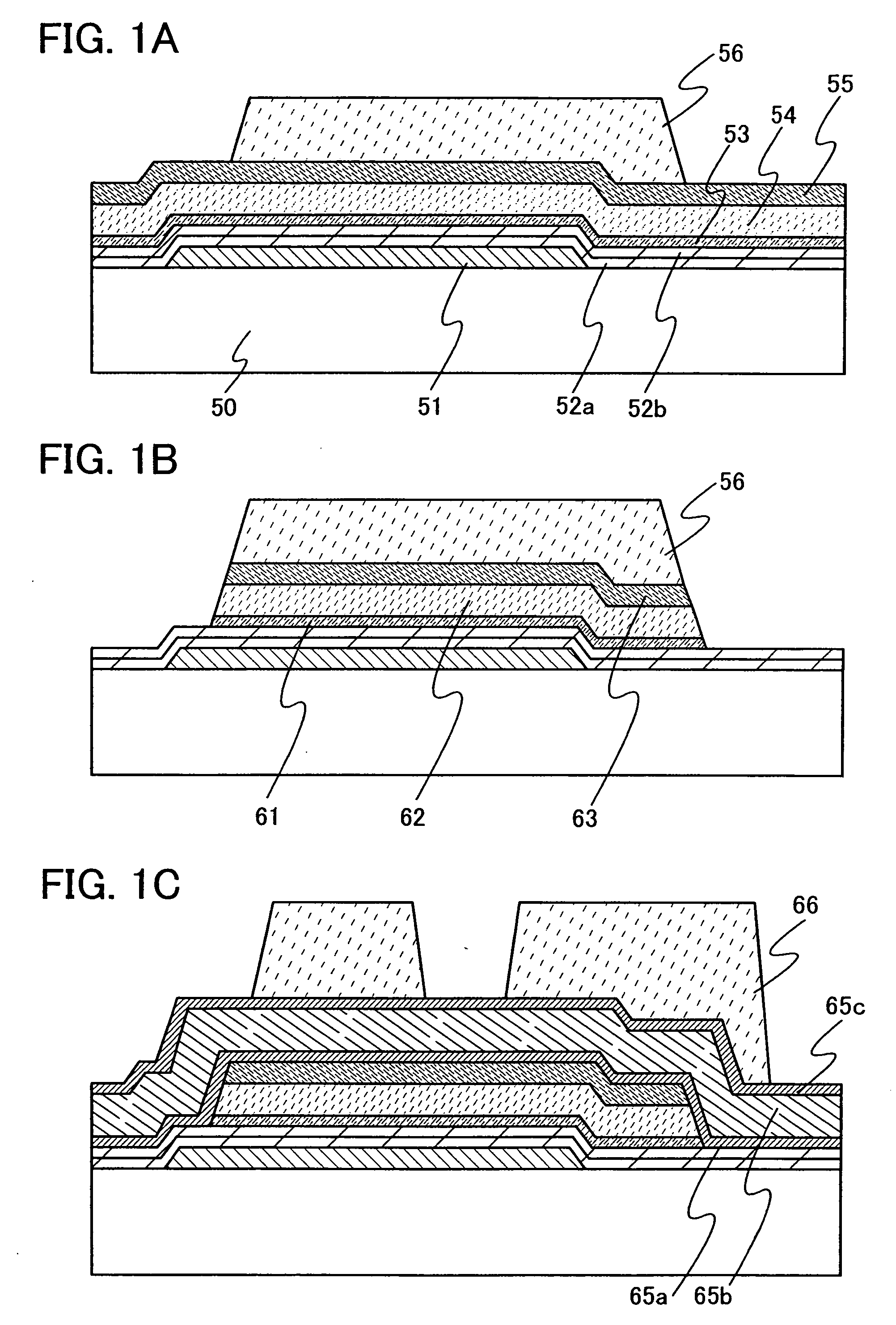
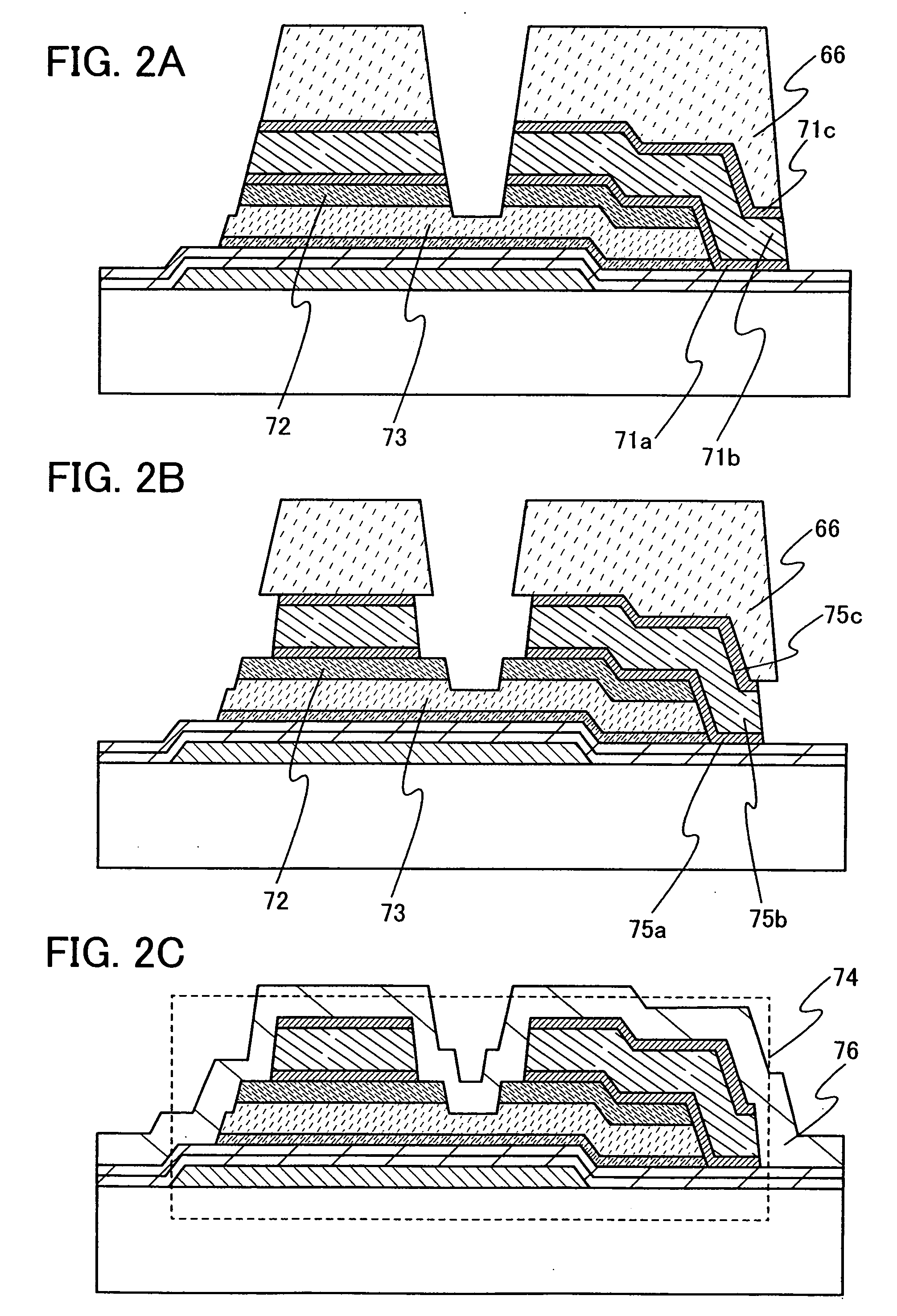
[0050]In this embodiment mode, manufacturing processes of thin film transistors used for a light-emitting device are described with reference to FIGS. 1A to 8D. FIGS. 1A to 3 and FIGS. 5A to 7 are cross-sectional views showing manufacturing processes of thin film transistors, and FIGS. 4A to 4C and FIGS. 8A to 8D are top views each showing a connection region of a thin film transistor and a pixel electrode in a single pixel.
[0051]A thin film transistor having a microcrystalline semiconductor film, which is of an n type, is more suitable for use in a driver circuit than that of a p type because it has a higher field-effect mobility. It is desired that all thin film transistors formed over the same substrate have the same polarity, in order to reduce the number of steps. Here, description is made using an n-channel thin film transistor.
[0052]As shown in FIG. 1A, a gate electrode 51 is formed over a substrate 50. As the substrate 50, any of the following substrates can be used: non-alk...
embodiment mode 2
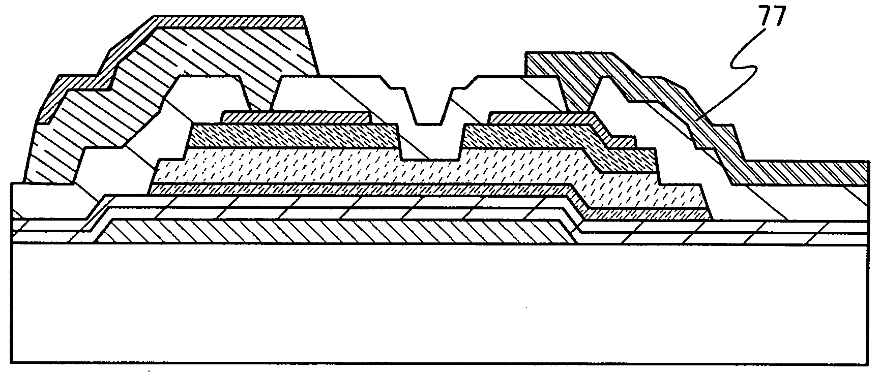
[0137]Next, a manufacturing process of a light-emitting device is described with reference to FIGS. 13A to 14C. A light-emitting device, in which a light-emitting element utilizing electroluminescence is used, is described here. Light-emitting elements utilizing electroluminescence are classified according to whether a light-emitting material is an organic compound or an inorganic compound. In general, the former is referred to as organic EL elements and the latter as inorganic EL elements. The manufacturing process of a thin film transistor, which is shown in FIGS. 5A to 8D, is used here, but the manufacturing process shown in FIGS. 1A to 3 can also be used appropriately.
[0138]In an organic EL element, by application of a voltage to a light-emitting element, electrons and holes are separately injected from a pair of electrodes into a layer containing a light-emitting organic compound, and a current flows. Then, recombination of these carriers (the electrons and holes) causes the li...
embodiment mode 3
[0160]Next, a structure of a light-emitting panel, which is one mode of a light-emitting device of the present invention, is described below.
[0161]FIG. 10A shows a mode of a light-emitting panel in which a signal line driver circuit 6013 which is separately formed is connected to a pixel portion 6012 formed over a substrate 6011. The pixel portion 6012 and a scan line driver circuit 6014 are each formed using a thin film transistor in which a microcrystalline semiconductor film is used. When the signal line driver circuit is formed using a transistor in which higher field-effect mobility can be obtained compared with the thin film transistor in which the microcrystalline semiconductor film is used, an operation of the signal line driver circuit which demands higher driving frequency than that of the scan line driver circuit can be stabilized. Note that the signal line driver circuit 6013 may be formed using a transistor using a single crystalline semiconductor, a thin film transisto...
PUM
 Abstract
Description
Claims
Application Information