Semiconductor package and semiconductor device using the same

a semiconductor and semiconductor technology, applied in the direction of semiconductor devices, semiconductor/solid-state device details, electrical apparatus, etc., can solve the problems of adverse influence on peripheral chips and electronic components, and achieve the effects of reducing the size of the devi

Inactive Publication Date: 2009-01-01
SHINKO ELECTRIC IND CO LTD
View PDF21 Cites 22 Cited by
  • Summary
  • Abstract
  • Description
  • Claims
  • Application Information

AI Technical Summary

Benefits of technology

[0036]According to the semiconductor package and the semiconductor device using the semiconductor package in accordance with the invention, even if the frame-shaped structure portion for preventing an underfill resin from flowing out in a semiconductor package having different connecting portions through a flip-chip connection and a BGA connection or an LGA connection and a semiconductor device using the semiconductor package, it ...

Problems solved by technology

When the size of the semiconductor chip itself is reduced and mounting densities of the semiconductor chip and other electronic components are inc...

Method used


Image

  • Semiconductor package and semiconductor device using the same
  • Semiconductor package and semiconductor device using the same
  • Semiconductor package and semiconductor device using the same

Examples


Embodiment Construction

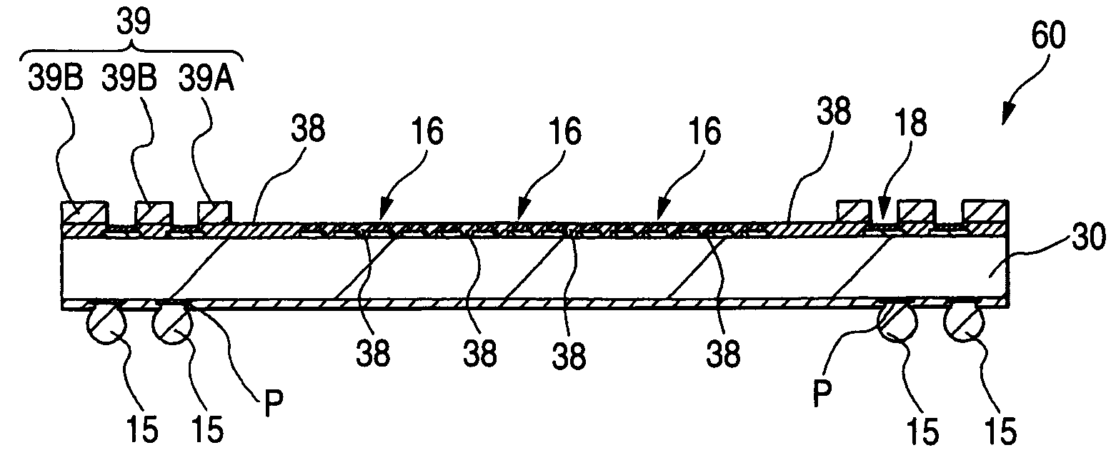
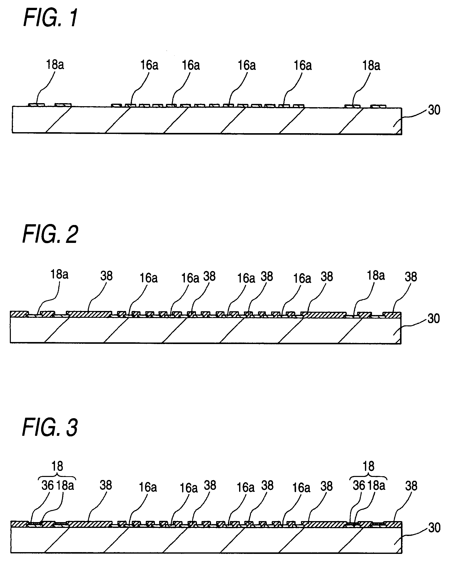
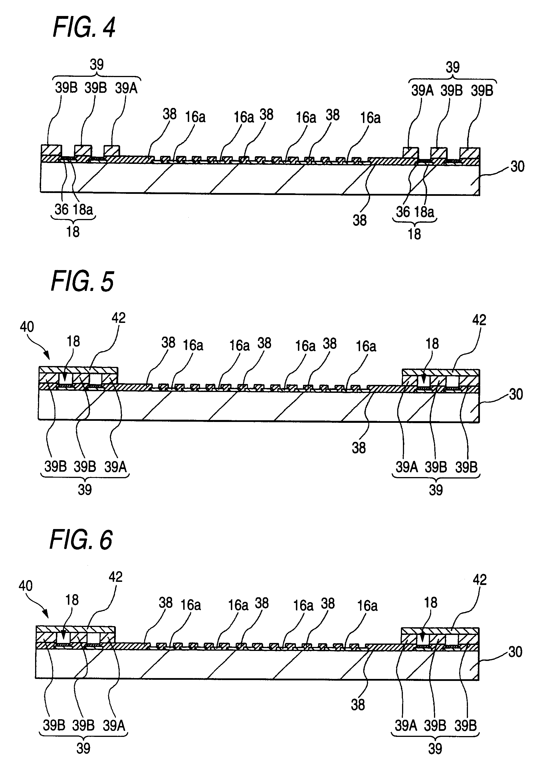
[0051]A preferred embodiment according to the invention will be described below in detail with reference to the accompanying drawings. FIGS. 1 to 10 are sectional views showing a process for manufacturing a semiconductor package according to the embodiment. FIG. 11 includes a plan view (FIG. 11A) showing a semiconductor package according to the embodiment and a sectional view (FIG. 11B) taken along an A-A line in the plan view. The sectional views in FIGS. 1 to 10 are taken along the A-A line in FIG. 11A.

[0052]FIG. 1 is a sectional view showing a state in which a resist pattern is formed on a resin substrate having a single side clad with copper. A resist pattern 34 is formed by cladding a resist film 33 to a copper foil 31 stuck to a resin substrate 30 and exposing and developing the resist film 33. The resist pattern 34 is formed to coat a predetermined wiring pattern which is not shown, and pattern portions of a flip-chip connecting pad 16 and a land pad 18 for carrying out a BGA...


PUM


Abstract

A semiconductor package 60 in which a region where a land pad 18 is formed is provided on an outer side of a region in which a flip-chip connecting pad 16 is formed, wherein a protecting member 39 is formed to expose the land pad 18 in the region in which the land pad 18 is formed, and the protecting member 39 includes a frame-shaped structure portion 39A disposed to surround the flip-chip connecting pad 16 and a support film portion 39B disposed on an outer side of the frame-shaped structure portion 39A, and a semiconductor device 70 using the semiconductor package 60.

Description

BACKGROUND OF THE INVENTION[0001]The present invention relates to a semiconductor package and a semiconductor device using the semiconductor package, and more particularly to a semiconductor package including a flip-chip connecting pad and a land pad to be used for a BGA (Ball Grid Array) or LGA (Land Grid Array) connection, and a semiconductor device using the semiconductor package.[0002]In a semiconductor package to be used for a portable telephone or a digital camera and a semiconductor device using the semiconductor package, an increase in a density and a reduction in a size have been desired. In an assembling technique of the semiconductor package and the semiconductor device which have densities increased and sizes reduced, a flip-chip connecting structure of a semiconductor chip is employed as effective means.[0003]In the flip-chip connecting structure, an interval between the semiconductor chip and a substrate of the semiconductor package in a chip mounting area is very smal...

Claims


Application Information

Patent Timeline
IPC IPC(8): H01L23/48
CPCH01L21/563H01L2224/26175H01L23/49816H01L23/49838H01L24/11H01L24/16H01L24/32H01L25/105H01L2224/13099H01L2224/16225H01L2224/27013H01L2224/73203H01L2224/73204H01L2224/83051H01L2224/83385H01L2924/01005H01L2924/01009H01L2924/01015H01L2924/01029H01L2924/01033H01L2924/01047H01L2924/0105H01L2924/01078H01L2924/01079H01L2924/15311H01L2924/15331H01L2924/3025H01L2224/32225H01L2924/01006H01L2924/014H01L2924/0132H01L23/3128H01L2224/29111H01L2225/1058H01L2225/1023H01L2224/2919H01L2924/1579H01L2924/3511H01L2924/00012H01L2924/00014
Inventor TAMADATE, YUKA
Owner SHINKO ELECTRIC IND CO LTD
Why Eureka
Try Eureka