Impedance adjusting circuit and semiconductor memory device having the same

a technology of impedance adjustment and semiconductor memory, applied in the field of impedance adjustment circuit, can solve the problems of impedance mismatch, output data distortion, signal reflectance to become more critical, etc., and achieve the effect of easy analysis of calibration operation

Inactive Publication Date: 2009-01-01
SK HYNIX INC
View PDF6 Cites 27 Cited by
  • Summary
  • Abstract
  • Description
  • Claims
  • Application Information

AI Technical Summary

Benefits of technology

[0026]Embodiments of the present invention are directed to providing an impedance adjusting circuit that can directly measure calibration resistance of the impedance adjusting circuit to easily analyze a calibration operation, and a semiconductor memory device having the impedance adjusting circuit.

Problems solved by technology

However, the reduction in the swing width of the signal has a great influence on an external noise, causing the signal reflectance to become more critical at an interface terminal due to impedance mismatch.
Such impedance mismatch is generally caused by an external noise, a variation of a power supply voltage, a change in an operating temperature, a change in a manufacturing process, etc.
The impedance mismatch may lead to a difficulty in high-speed transmission of data and distortion in output data.
Therefore, if semiconductor devices receive the distorted output signal through an input terminal, it frequently gives rise to problems such as a setup / hold failure and an error in decision of an input level.
However, mismatch exists between the resistors due to process variation or the like.
That is, the termination resistance can be measured by directly connecting a DQ pin to the termination resistor but there is no way to measure the resistance of the calibration resistor.
In particular, it is difficult to measure an internal voltage level after being packaged, which may lead to more serious problems.
That is, the conventional impedance adjusting circuit has a problem in that it is not easy to find out which portion of the impedance adjusting circuit gives rise to a trouble when the ZQ calibration does not normally operate.

Method used


Image

  • Impedance adjusting circuit and semiconductor memory device having the same
  • Impedance adjusting circuit and semiconductor memory device having the same
  • Impedance adjusting circuit and semiconductor memory device having the same

Examples


Embodiment Construction

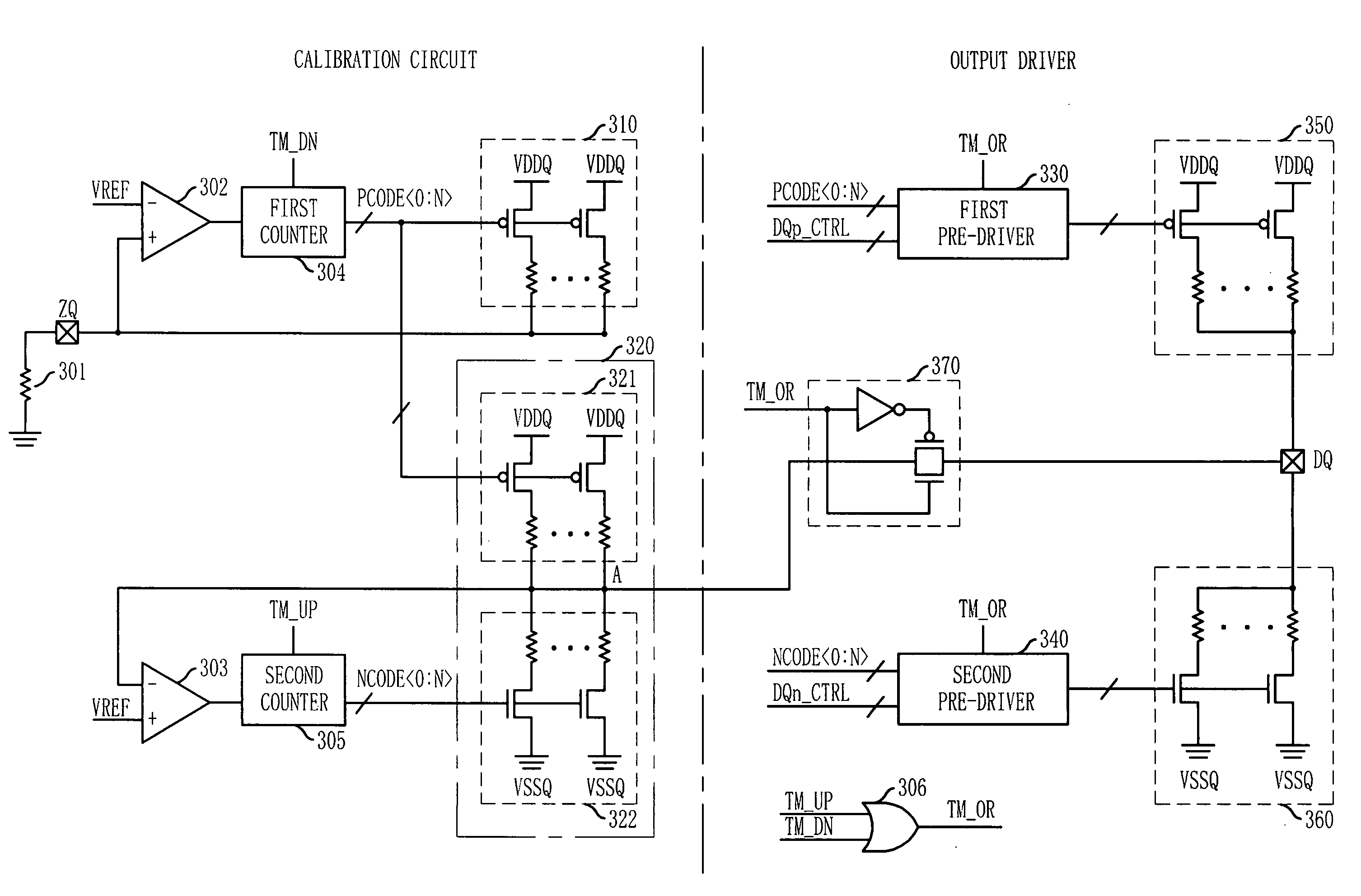
[0033]Hereinafter, an impedance adjusting circuit and a semiconductor memory device having the same in accordance with the present invention will be described in detail with reference to the accompanying drawings.

[0034]FIG. 3 is a block diagram of an impedance adjusting circuit applied to a semiconductor memory device in accordance with an embodiment of the present invention.

[0035]Referring to FIG. 3, the impedance adjusting circuit of the present invention includes first and second comparators 302 and 303, first and second counters 304 and 305, a first calibration resistor circuit 310, a second calibration resistor circuit 320, and a transmission line circuit 370. The first calibration resistor circuit is calibrated with an external resistor 301 and generates a first calibration code PCODE. The second calibration resistor circuit 320 is calibrated with the first calibration resistor circuit 310 and generates a second calibration code NCODE, the second calibration resistor circuit 3...


PUM


Abstract

An impedance adjusting circuit includes: a first calibration resistor circuit configured to be calibrated with an external resistor and generate a first calibration code; a second calibration resistor circuit configured to be calibrated with the first calibration resistor circuit and generate a second calibration code, the second calibration resistor circuit being connected to a first node; and a transmission line circuit configured to be responsive to a control signal to connect the first node to a pin of a system employing the impedance adjusting circuit.

Description

CROSS-REFERENCE TO RELATED APPLICATIONS[0001]The present invention claims priority of Korean patent application number 10-2007-0063312, filed on Jun. 26, 2007, which is incorporated by reference in its entirety.BACKGROUND OF THE INVENTION[0002]The present invention relates to an impedance adjusting circuit used in various integrated circuits such as a semiconductor memory device, and more particularly, to an impedance adjusting circuit configured to easily measure an offset value.[0003]Semiconductor devices are implemented into integrated circuit (IC) chips such as central processing units (CPUs), memories, and gate arrays, and are incorporated into a variety of electrical products such as personal computers, servers and workstations. Most semiconductor devices include a receiving circuit configured to receive signals from an outside world via input pads and an output circuit configured to provide internal signals to an outside world via output pads.[0004]As the operating speed of e...

Claims


Application Information

Patent Timeline
Patent Type & Authority Applications(United States)
IPC IPC(8): H03K19/003
CPCH04L25/028G11C7/10H01L27/02
Inventor JEONG, CHUN-SEOKLEE, KANG-SEOL
Owner SK HYNIX INC
Why Eureka
Try Eureka