Solid-state imaging device and camera module

a technology of solid-state imaging and camera module, which is applied in the direction of radio frequency controlled devices, instruments, television systems, etc., can solve the problems of reducing sensitivity or the like, and achieve the effect of suppressing the appearance of color mixtures and high-quality images

Active Publication Date: 2009-01-01
SONY CORP
View PDF2 Cites 53 Cited by
  • Summary
  • Abstract
  • Description
  • Claims
  • Application Information

AI Technical Summary

Benefits of technology

[0018]According to the solid-state imaging device of the embodiment of the present invention, oblique incident light is blocked by the side wall of the optical inner filter layer and suppressed so as not to enter adjacent pixels. As a result, the occurrence of a color mixture can be suppressed. The camera module according to the embodiment of the present invention includes the above solid-state imaging device, so that the occurrence of a color mixture can be suppressed while obtaining high quality images.

Problems solved by technology

Thus, it may result in a decrease in sensitivity or the like.

Method used


Image

  • Solid-state imaging device and camera module
  • Solid-state imaging device and camera module
  • Solid-state imaging device and camera module

Examples


first embodiment

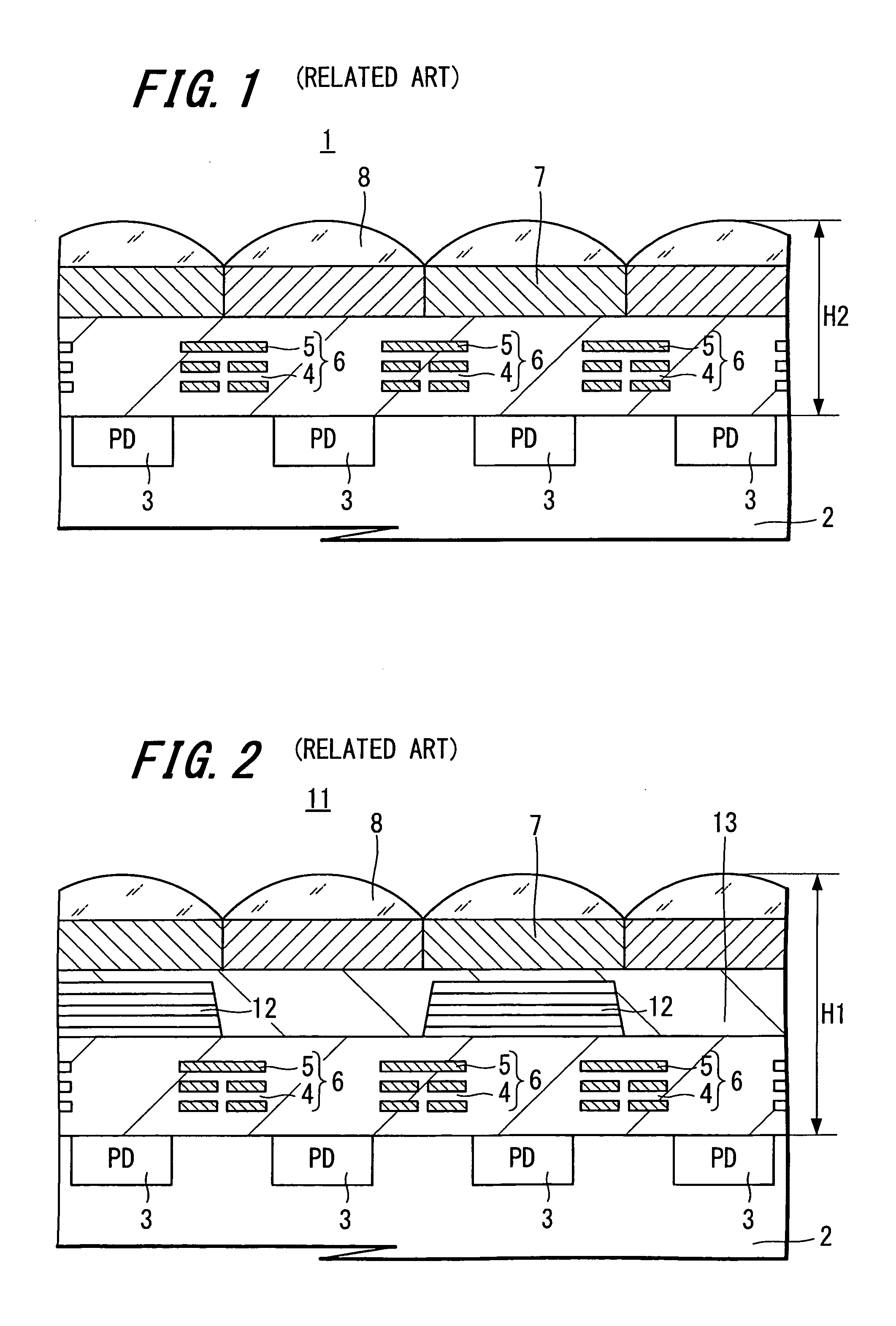
[0055]Next, FIG. 6 illustrates a cross-sectional structure of the main parts of a CMOS solid-state imaging device in accordance with the present invention. In order to describe an embodiment of the present invention in a straightforward manner, a pixel is represented only by a photodiode PD and is schematically described while omitting pixel transistors. The same will be applied to each of other embodiments described later.

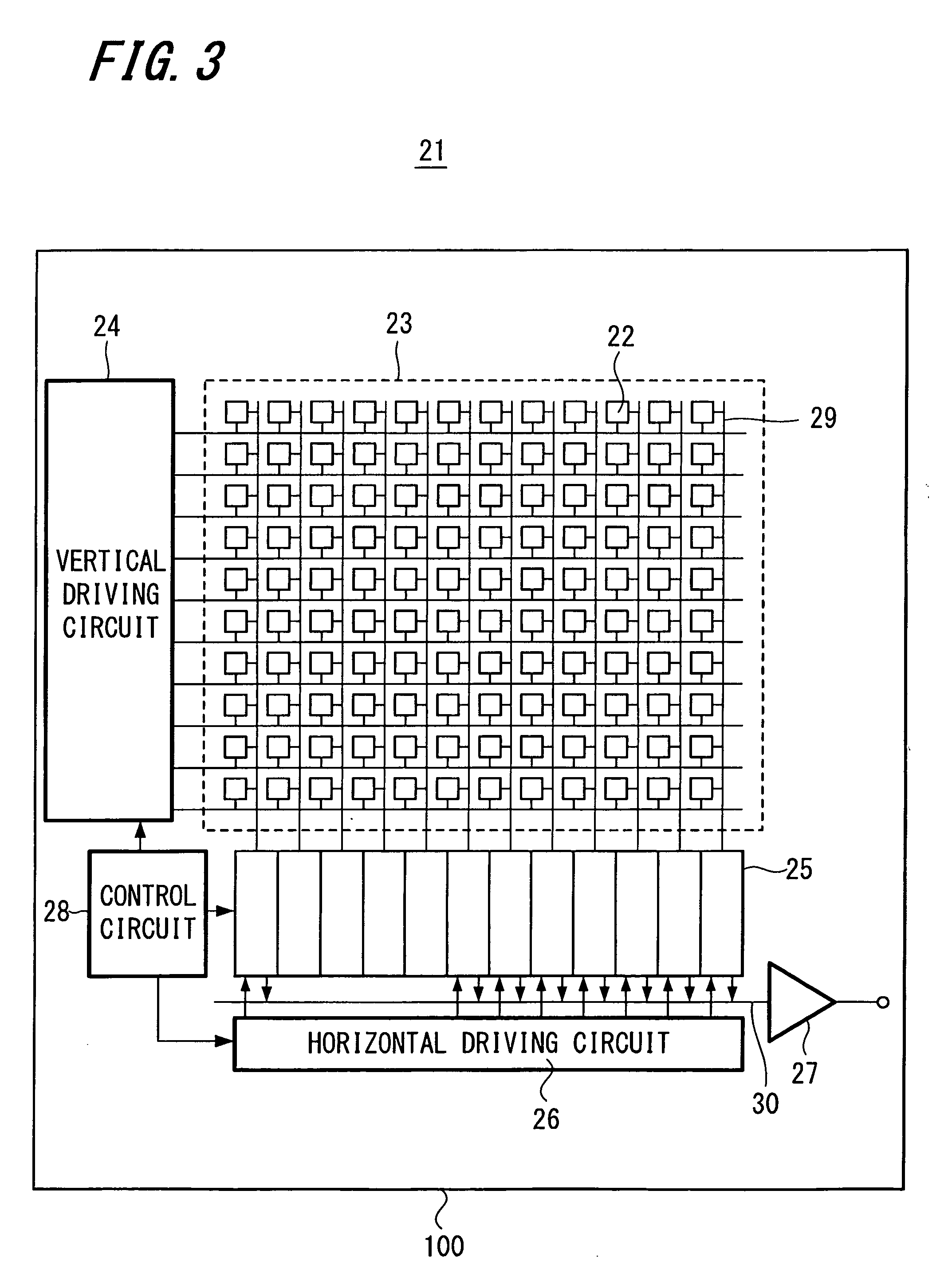
[0056]As shown in FIG. 6, the CMOS solid-state imaging device 61 in accordance with the first embodiment includes a plurality of pixels 22, each having the photodiode (PD) 31, arranged in a two-dimensional array on the principal surface of a semiconductor substrate 100. In addition, a plurality of layers is formed on the semiconductor substrate 100 through an insulating interlayer 53. In this example, three layered lines 54 [541, 542, and 543] form a plurality of wiring layers 55. An optical inner filter layer 62 for blocking infrared light is formed above the plu...

second embodiment

[0068]FIG. 11 illustrates a CMOS solid-state imaging device in accordance with the present invention. This CMOS solid-state imaging device is provided with the inner-layer lens 82 shown in FIG. 10. In the CMOS solid-state imaging device 67 of the present embodiment, an optical inner filter layer (IR cut filter layer) 62 is formed between the plurality of wiring layers 55 and the color filter 65, corresponding to a desired pixel. In addition, a side wall 63 with a light-blocking effect (in this example, a side wall formed of a metal film) is formed on the lateral wall of the optical inner filter layer 62. Then, a downwardly-convexed inner-layer lens 82 as shown in FIG. 10 is formed on the interlayer between the optical inner filter layers 62 adjacent to each other, corresponding to the photodiode 31 of the IR pixel. The inner-layer lens 82 includes a first interlayer 83 (in this example, a BPSG film) and a second interlayer 84 (in this example, a silicon nitride film) having a refrac...

third embodiment

[0081]FIG. 16 illustrates a CMOS solid-state imaging device in accordance with the present invention. The CMOS solid-state imaging device 94 of the present embodiment is provided with an optical inner filter layer 62 (IR cut filter layer) formed between a plurality of wiring layers 55 and a color filter 65, corresponding to a desired pixel. On the lateral wall of the optical inner filter layer 62, a side wall 63 with a light-blocking effect (in the present example, a side wall formed of a metal film) is formed. Furthermore, the CMOS solid-state imaging device 94 includes a downwardly-convexed inner-layer lens 95 formed with two layers with different refractive indexes in an interlayer between a plurality of wiring layers 55 where no layered lines 54 [541 to 543] are formed. Specifically, the downwardly-convexed inner-layer lens 95 is formed by using an insulating interlayer 53 on the area between layered lines 54 adjacent to each other, corresponding to each of the photodiodes (PDs)...


PUM


Abstract

A solid-state imaging device is provided. The solid-state imaging device includes a plurality of arrayed pixels, an optical inner filter layer, and a light-blocking side wall. The plurality of arrayed pixels each includes a photoelectric conversion portion and a pixel transistor. The optical inner filter layer is provided for blocking infrared light and formed facing toward a light-receiving surface of the photoelectric conversion portion of a desired pixel among the arrayed pixels. The light-blocking side wall is formed on a lateral wall of the optical inner filter layer.

Description

CROSS REFERENCES TO RELATED APPLICATIONS[0001]The present invention contains subject matter related to Japanese Patent Application JP 2007-171008 filed in the Japanese Patent Office on Jun. 28, 2007, the entire contents of which are incorporated herein by reference.BACKGROUND OF THE INVENTION[0002]1. Field of the Invention[0003]The present invention relates to a solid-state imaging device, particularly, a solid-state imaging device, for example, a MOS image sensor in which a photoelectric conversion portion and a pixel transistor are included in a pixel. In addition, the present invention relates to a camera module including such a solid-state imaging device.[0004]2. Description of the Related Art[0005]Solid-state imaging devices can be roughly classified into charge transfer solid-state imaging devices typified by CCD image sensors and amplified solid-state imaging devices typified by CMOS image sensors. In comparison with the CMOS image sensor, the CCD image sensor may need a powe...

Claims


Application Information

Patent Timeline
Patent Type & Authority Applications(United States)
IPC IPC(8): H04N5/335H04N5/225G02B7/02G03B30/00H01L27/14H01L27/146H04N5/357H04N5/369H04N5/374H04N5/3745
CPCH01L27/14621H01L27/14685H01L27/14643H01L27/14627H01L27/14623H01L27/14612H01L27/14625H01L27/14636H01L27/14641H01L27/146H04N25/00
Inventor GODAIIN, HIRONORI
Owner SONY CORP
Why Eureka
Try Eureka