Image Display Device

Inactive Publication Date: 2009-01-01
HITACHI LTD
View PDF3 Cites 10 Cited by
  • Summary
  • Abstract
  • Description
  • Claims
  • Application Information

AI Technical Summary

Benefits of technology

[0021]According to the first aspect of the invention, the influence of the electric field distortions in the outside the front substrate is shielded by the first translucent conductive layer, thus the potential variation can be prevented form being transferred to the inside of the vacuum panel, and consequently, there can be obtained an extremely preferable advantage that the abnormal discharge in the vacuum panel can be prevented, and the image display device having high quality and reliability, and longer life can be realized.
[0022]Further, according to the second aspect of the invention, when the abnormal d

Problems solved by technology

Further, the gap between the opposed inside surfaces of the front substrate and the rear surface is in a range of about 1 mm through 3 mm, and abnormal discharge is caused between the opposed surfaces by turbulence in the electric field, etc.
As one of the causes of inducing the abnormal discharge, there can be cited accumulation of electr

Method used


Image

  • Image Display Device
  • Image Display Device
  • Image Display Device

Examples


first embodiment

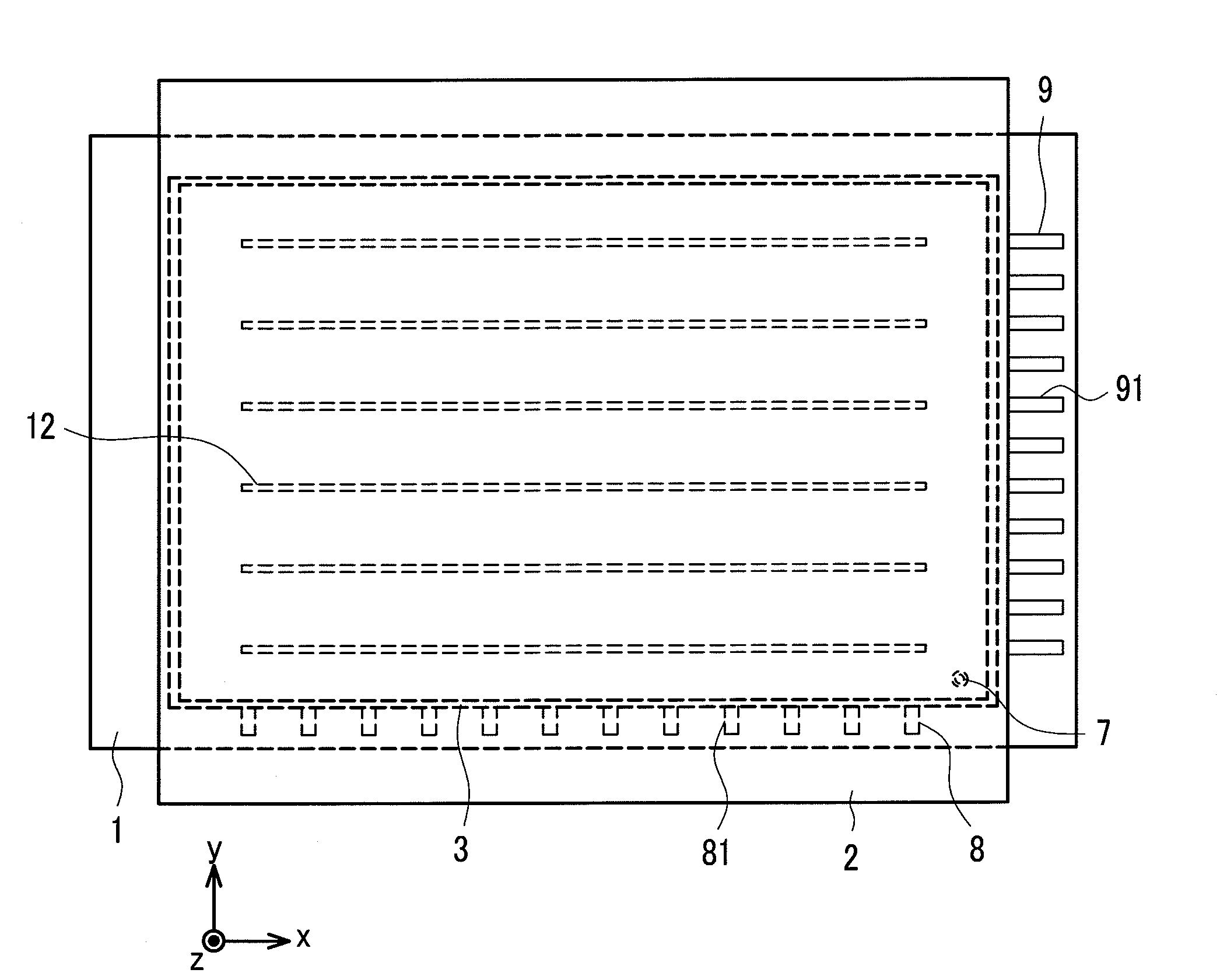
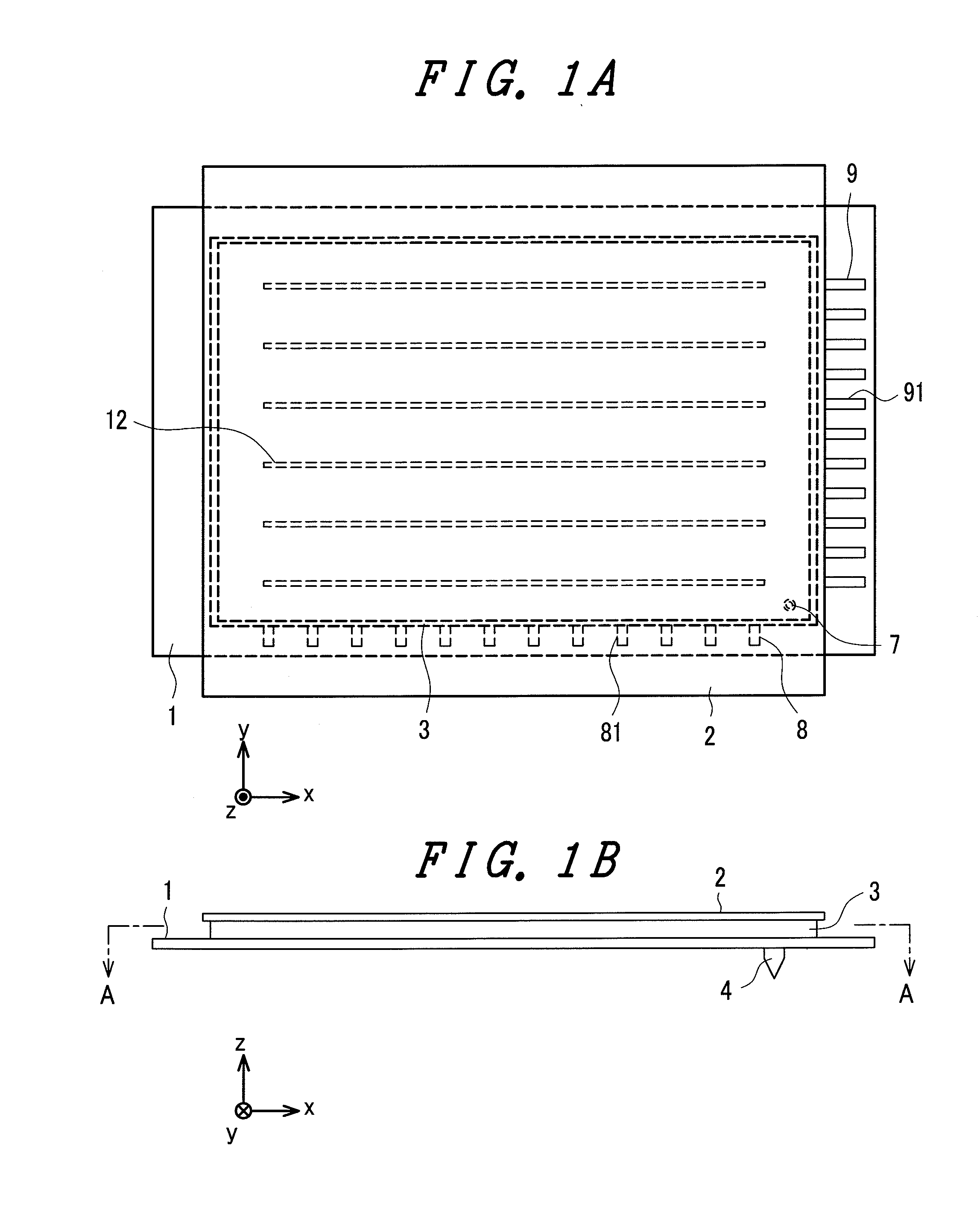
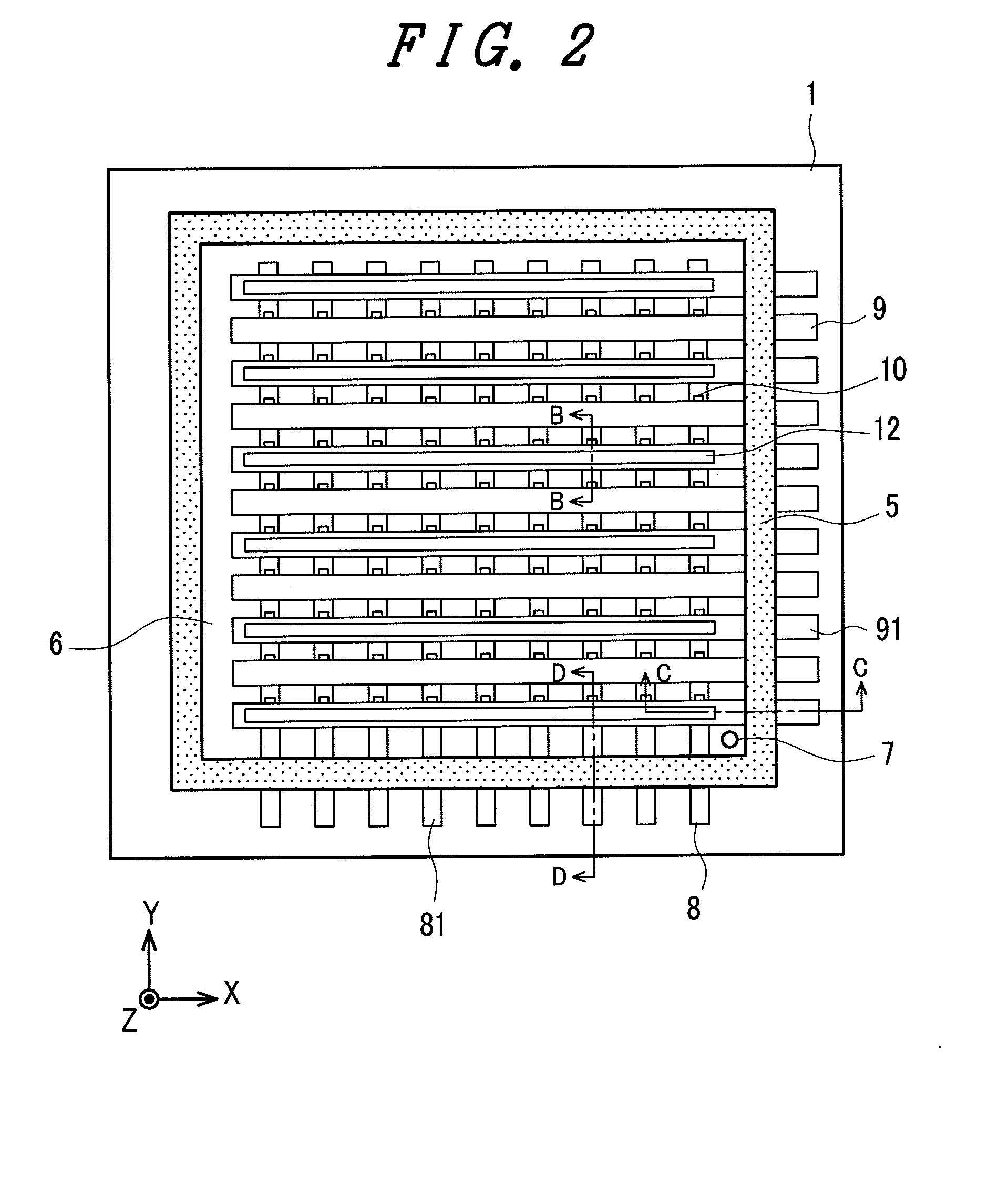
[0033]FIGS. 1A, 1B, and 2 through 4 are schematic diagrams for explaining a first embodiment of the image display device according to the invention, wherein FIG. 1A is a plan view viewed from a front substrate side, FIG. 1B is a side view of FIG. 1A, FIG. 2 is a plan view along the A-A line shown in FIG. 1B, FIG. 3 is a cross-sectional view along the B-B line shown in FIG. 2, FIG. 4 is a cross-sectional view along the C-C line shown in FIG. 2, and FIG. 5 is a cross-sectional view along the D-D line shown in FIG. 2.

[0034]In FIGS. 1A, 1B, and 2 through 5, the reference numeral 1 denotes a rear substrate, the reference numeral 2 denotes a front substrate, the reference numeral 3 denotes a frame member, the reference numeral 4 denotes an evacuation tube, the reference numeral 5 denotes a seal member, the reference numeral 6 denotes a display area, the reference numeral 7 denotes a through hole, the reference numeral 8 denotes picture signal lines, the reference numeral 9 denotes scannin...

second embodiment

[0052]FIG. 8 is an enlarged diagram of a substantial part of the display panel showing another embodiment of the image display device according to the invention, wherein the same parts as in the drawings described above will be denoted with the same reference numerals, and the explanations therefor will be omitted. FIG. 8 is different from FIG. 6 in that the first translucent conductive layer 18 formed on the front surface side of the front substrate 2 has a function as a voltage applying layer. Further, as shown in FIG. 9 with the schematic diagram thereof, a low voltage power supply Vb having a voltage lower than that of the high voltage power supply Va is connected to the first translucent conductive layer 18.

[0053]According to the configuration of the second embodiment, the first translucent conductive layer 18 as the voltage applying layer is formed on the outside surface of the front substrate 2, and the surface of the front substrate is grounded by the second translucent cond...


PUM


Abstract

A first translucent conductive layer is disposed on a front surface of a front substrate, a translucent insulating member is disposed on a front surface of the first translucent conductive layer, and a second translucent conductive layer held at the ground potential is disposed on a front surface of the translucent insulating member. According to the invention, an image display device, which prevents the abnormal discharge in the vacuum panel from occurring, and has high quality and reliability and long life, can be provided.

Description

CROSS-REFERENCE TO RELATED APPLICATION[0001]The present application claims priority from Japanese application JP2007-151188 filed on Jun. 7, 2007, the content of which is hereby incorporated by reference into this application.BACKGROUND OF THE INVENTION[0002]1. Technical Field[0003]The present invention relates to a light emitting flat panel image display device, and in particular to an image display device having electron sources arranged in a matrix.[0004]2. Related Art[0005]As an example of a light emitting flat panel display (FPD) having electron sources arranged in a matrix, there are known a field emission display (FED) and an electron emitter display using microscopic cold cathodes suitable for integration. As such cold cathodes, there can be cited electron sources such as a Spindt type electron source, a surface-conduction electron source, a carbon nanotube electron source, a metal-insulator-metal (MIM) type having metal-insulator-metal layers, a metal-insulator-semiconducto...

Claims


Application Information

Patent Timeline
IPC IPC(8): H04N5/66
CPCH01J29/867H01J29/88H01J2329/92H01J31/123H01J2329/869H01J29/92
Inventor HOSOTANI, NOBUHIKOTACHIBANA, TADAYOSHIKATO, TATSURO
Owner HITACHI LTD
Why Eureka
Try Eureka