Semiconductor device, lead frame, and manufacturing method for the lead frame

a semiconductor and lead frame technology, applied in the direction of printed circuit, sustainable manufacturing/processing, final product manufacturing, etc., can solve the problems of lead-tip portion prone to be affected, low mounting strength against a circuit board, etc., to improve strength, improve mounting strength, and improve solder wettalibity

Inactive Publication Date: 2009-01-08
ABLIC INC
View PDF3 Cites 10 Cited by
  • Summary
  • Abstract
  • Description
  • Claims
  • Application Information

AI Technical Summary

Benefits of technology

[0008]In order to firmly bond a lead of a semiconductor device with an electrode of a circuit board, there is provided a semiconductor device having a lead in which plating covers entirely a lead-tip portion of the semiconductor device as means for improving solder wettalibity in the lead of the semiconductor device. Further, as another means, there is provided a semiconductor device having a lead in which an area of a lead-tip cut portion on which plating is not formed is less than half of a cross-sectional area of the lead of the semiconductor device.
[0009]According to the present invention, a molten soldering material melted by heat generated in reflow goes up the lead to the upper surface thereof, whereby mounting strength to a circuit board can be improved without enlarging the lead area of the semiconductor device. Further, it is possible to improve strength with respect to warpage or the like of the circuit board on which the semiconductor device is mounted.

Problems solved by technology

However, along with the miniaturization of a semiconductor device, the mounting strength against a circuit board tends to be lower.
This is because the lead-tip portion is apt to be affected by influence such as warpage of the circuit board when the semiconductor device is mounted onto the circuit board.

Method used


Image

  • Semiconductor device, lead frame, and manufacturing method for the lead frame
  • Semiconductor device, lead frame, and manufacturing method for the lead frame
  • Semiconductor device, lead frame, and manufacturing method for the lead frame

Examples


first embodiment

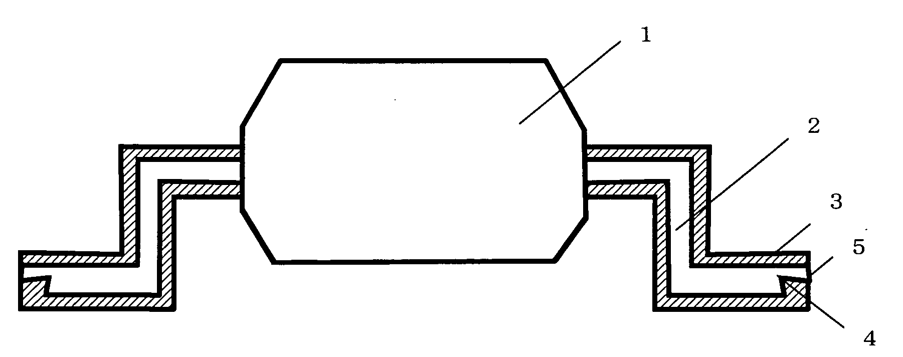
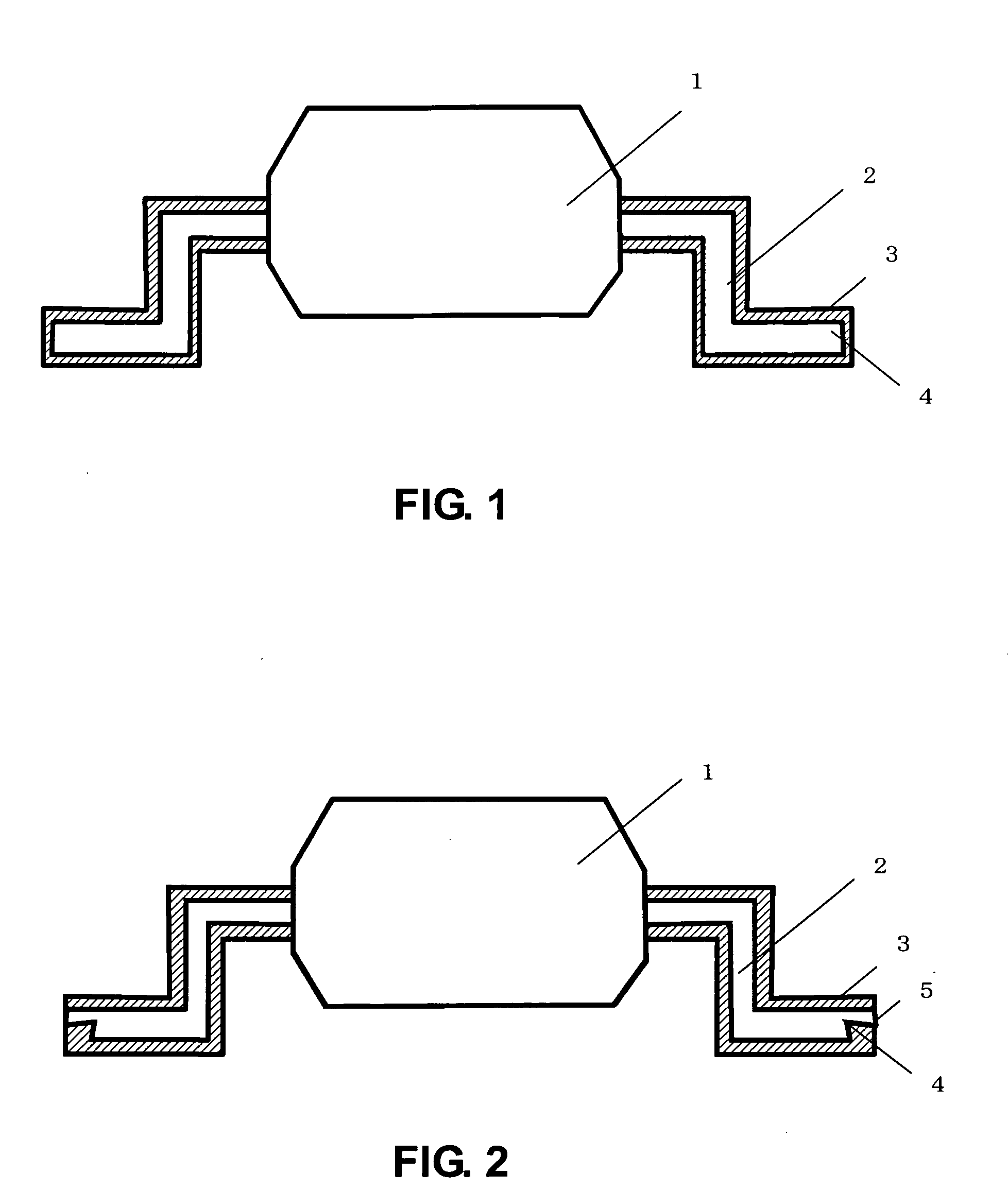
[0021]FIG. 1 is a schematic cross-sectional view showing a structure of a semiconductor device of the present invention. The semiconductor device includes a resin 1, a lead 2, and a metal plating layer 3 covering the surface of the lead 2. Since elements including a semiconductor integrated circuit (IC chip) are covered by the resin 1, the elements can not be seen from outside thereof generally. One end of the lead 2 is electrically connected to the semiconductor integrated circuit inside the resin 1, and another end thereof protrudes from the resin 1. The protruding portion of the lead 2 is formed into a shape suitable for mounting onto a substrate by the use of a die or the like. The plating layer 3 is formed on the entire surface of a portion of the lead 2 which is exposed to the outside of the resin 1. In the embodiment shown in FIG. 1, the plating layer 3 covers a lead-tip portion 4 of the lead 2 at an end portion thereof so that no surface of the lead is exposed to the outside...

second embodiment

[0022]FIG. 2 is a schematic cross-sectional view showing a structure of a semiconductor device of the present invention. In the embodiment shown in FIG. 2, the lead-tip portion of the lead 2 has a portion covered by the plating layer 3, and a lead-tip end surface 5 not covered by the plating layer 3. A cross-sectional area of the lead-tip end surface 5 is made smaller than a half of the cross-sectional area of the lead 2. Consequently, at the time of mounting the semiconductor device onto a circuit board or the like, it is easy for a soldering material to wet the plating layer, permitting the solder to go up the lead-tip portion to form a rigid mounting state.

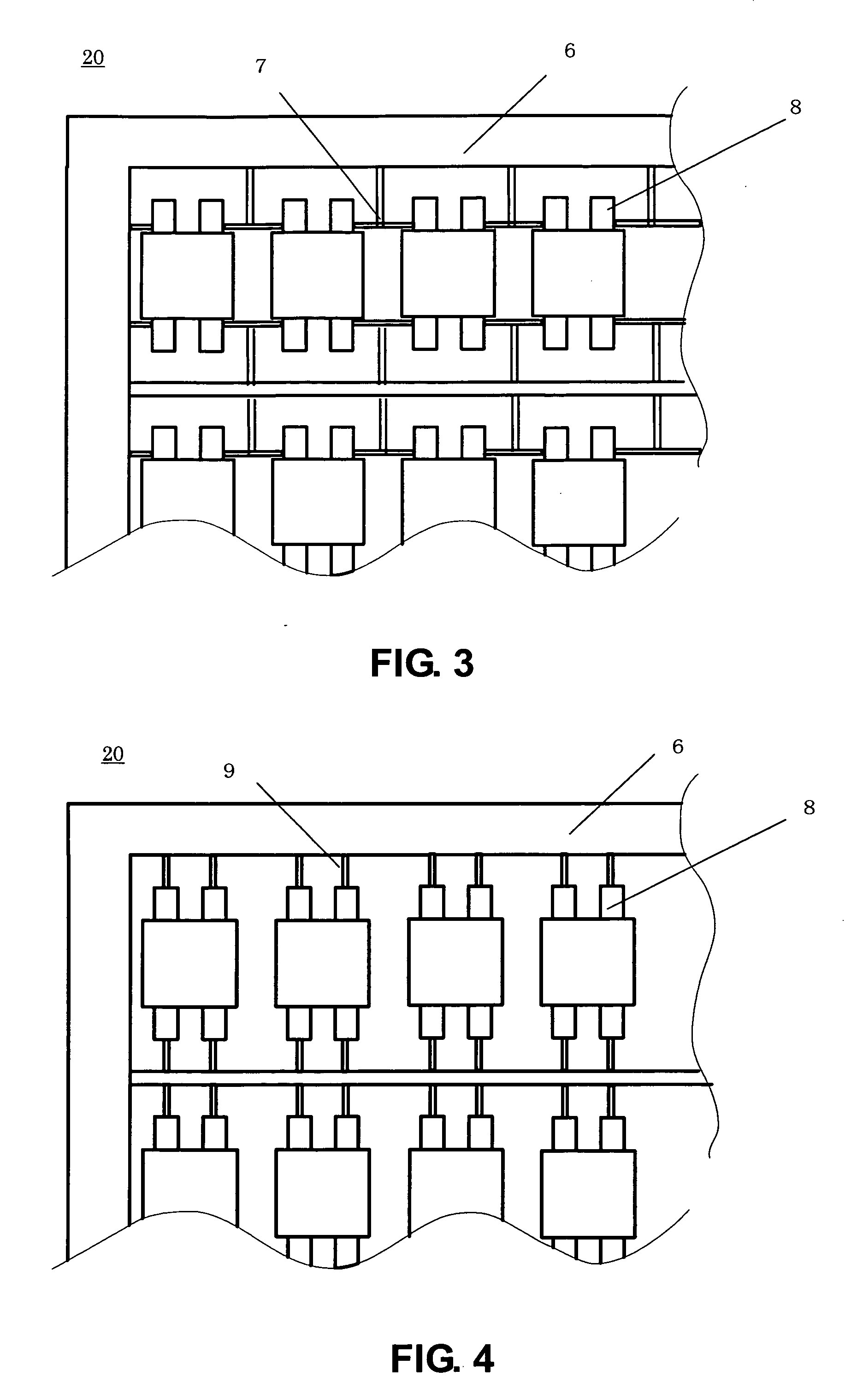
[0023]FIG. 3 shows a first embodiment of a lead frame according to the present invention, that is, shows an aggregate in which a plurality of semiconductor devices are arranged on a single lead frame 20. A lead 8 of each of the semiconductor devices is connected to another lead 8 by a plating bar 7, and the plating bar 7 is joi...


PUM

PropertyMeasurementUnit
areaaaaaaaaaaa
thicknessaaaaaaaaaa
strengthaaaaaaaaaa

Abstract

Provided is a semiconductor device having an element covered with a resin mold and a metal lead protruding from the resin mold in which a lead-tip portion thereof is entirely covered by solder plating and in which a lead-tip end surface, which is not covered by solder plating, has an area less than half of a cross-sectional area of the metal lead, whereby solder wettability of the metal lead is improved and a bonding strength to a circuit board is also improved.

Description

BACKGROUND OF THE INVENTION[0001]1. Field of the Invention[0002]The present invention relates to a semiconductor device manufactured by molding an element such as a semiconductor integrated circuit mounted on a lead frame with resin, and to a manufacturing method for the lead frame.[0003]2. Description of the Related Art[0004]A semiconductor device in which an element such as a semiconductor integrated circuit mounted on a lead frame is molded with resin is generally mounted onto a circuit board for use. In order to ensure sufficient mounting strength between the semiconductor device and the circuit board, leads of the semiconductor device are elongated to enlarge soldering area. Though solder wettability in a cut surface of leads of the semiconductor device, conventionally, has not been kept in good condition, large soldering area and Z-shaped forming of the leads make the solder wettability not only in both ends of the lead but also in heel portions of the leads good, permitting t...

Claims


Application Information

Patent Timeline
Patent Type & Authority Applications(United States)
IPC IPC(8): H01L23/495H01L21/00
CPCH01L23/49582H05K3/3426H05K2201/10689H05K2201/10795H01L2924/0002H05K2201/10909H01L2924/00Y02P70/50H01L23/495
Inventor YOSHINO, TOMOYUKI
Owner ABLIC INC
Why Eureka
Try Eureka