
Local Oxidation of Silicon Planarization for Polysilicon Layers Under Thin Film Structures

a technology of polysilicon and thin film structure, applied in the direction of fixed capacitor details, variable capacitors, fixed capacitors, etc., can solve the problems of significant problems in the subsequent formation and patterning of layers, and achieve the effect of reducing or eliminating problems and high yield manufacturing

Active Publication Date: 2009-01-15
NXP USA INC
View PDF13 Cites 25 Cited by
  • Summary
  • Abstract
  • Description
  • Claims
  • Application Information

AI Technical Summary

Benefits of technology

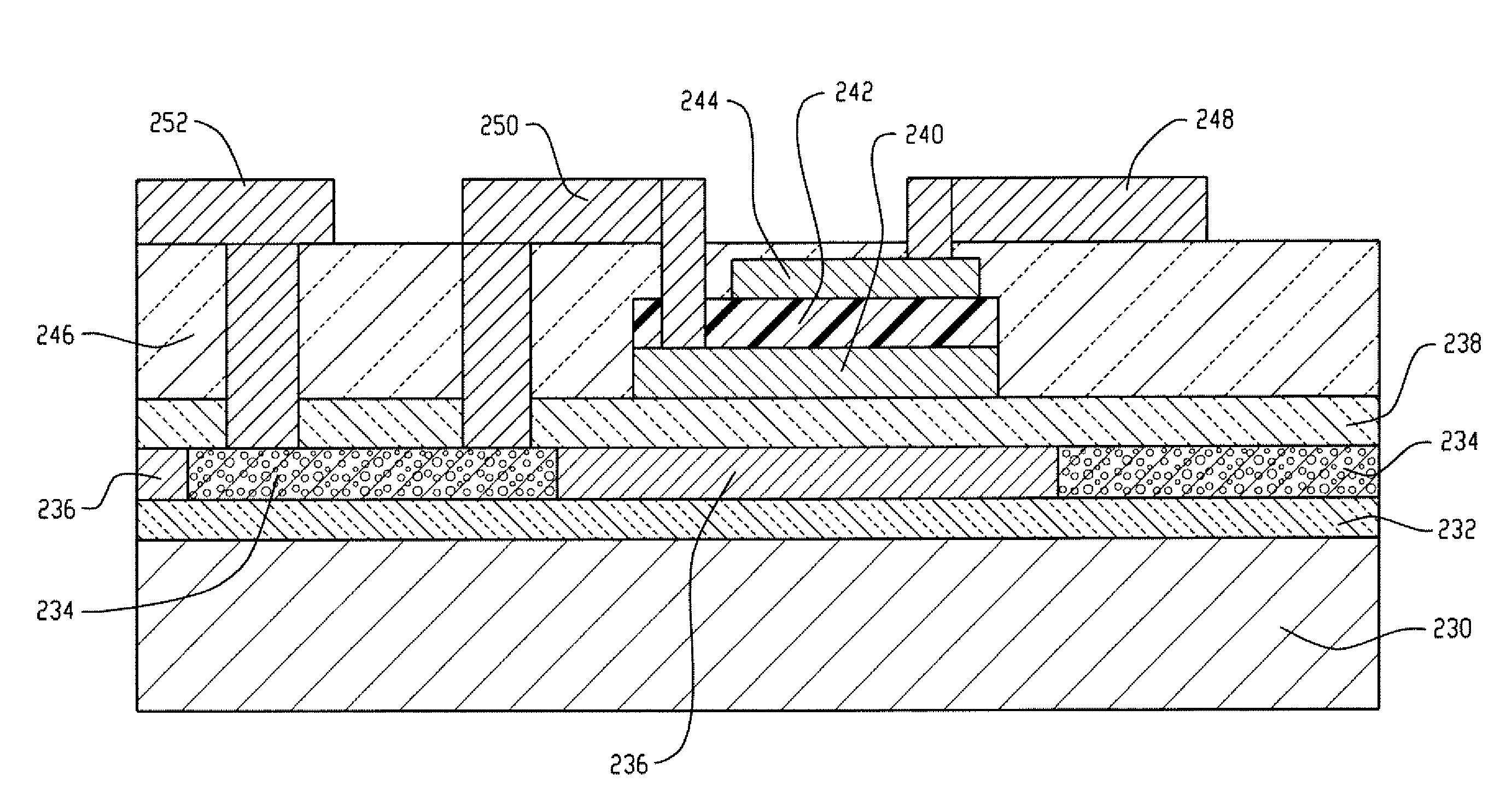
[0001]Thin film devices, such as micro-electromechanical systems (MEMS) and thin film capacitors, typically require an atomically smooth surface for high yield manufacturing. These thin film devices are generally made from layers deposited and patterned in a series of successive steps, one layer at a time, that build up the final device structure. The topography created on the surface by underlying patterned films, such as polysilicon, can cause significant problems for the subsequent formation and patterning of layers, such as stringers, striations in spin-on films and focus problems in photolithography. Previous efforts to reduce these and other problems associated with depositing thin film layers on top of a patterned polysilicon have included limiting the thickness of the polysilicon layer, typically to 1 um. It would be advantageous to provide an extremely planar surface on a patterned polysilicon layer in order to reduce or eliminate the problems associated with forming layers on top of patterned films.

Problems solved by technology

The topography created on the surface by underlying patterned films, such as polysilicon, can cause significant problems for the subsequent formation and patterning of layers, such as stringers, striations in spin-on films and focus problems in photolithography.

Method used


Image

  • Local Oxidation of Silicon Planarization for Polysilicon Layers Under Thin Film Structures
  • Local Oxidation of Silicon Planarization for Polysilicon Layers Under Thin Film Structures
  • Local Oxidation of Silicon Planarization for Polysilicon Layers Under Thin Film Structures

Examples


Embodiment Construction

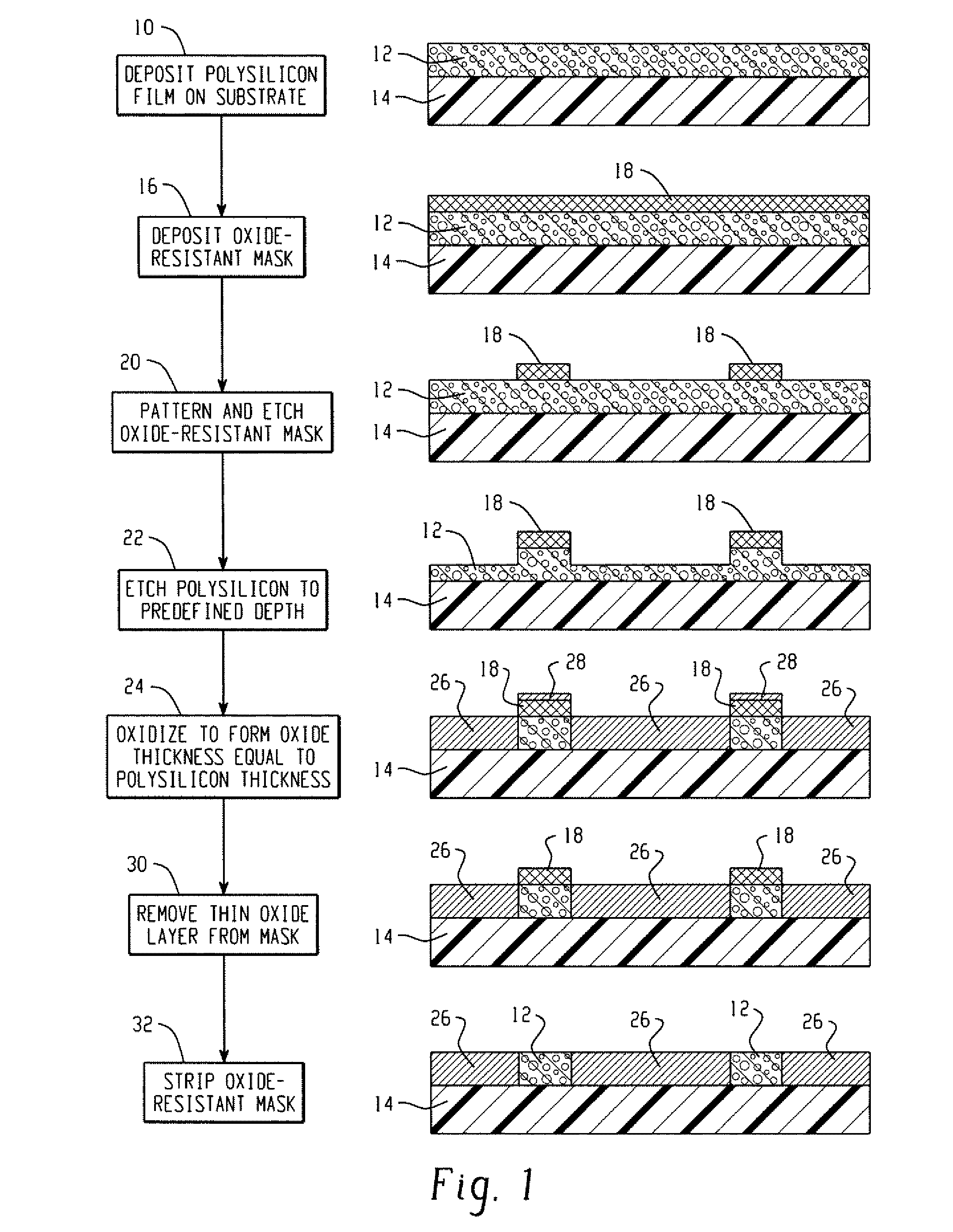
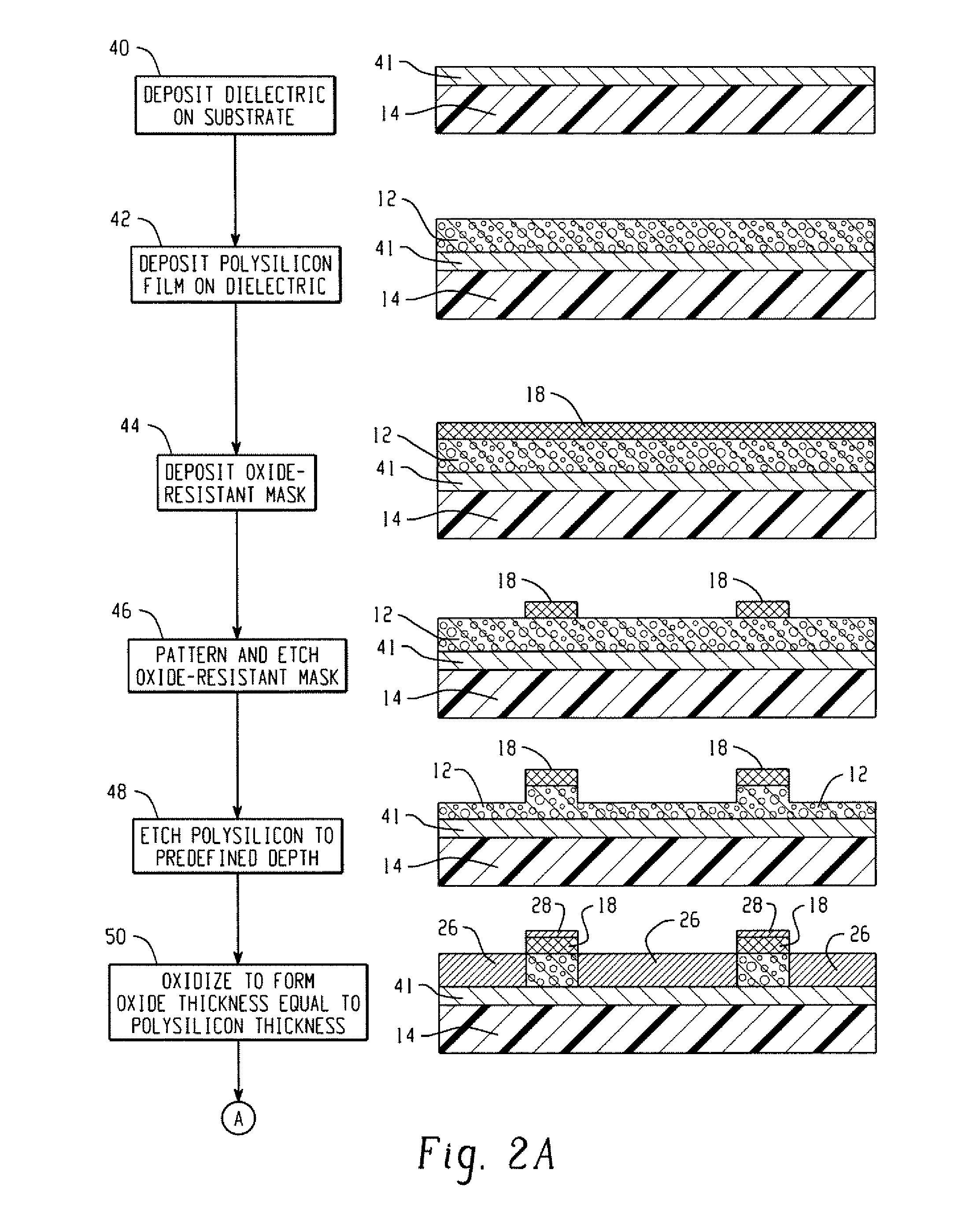
[0011]FIG. 1 depicts an example process for fabricating a patterned polysilicon layer having a planar surface. The steps of the process are illustrated on the left-hand side of FIG. 1, and examples of the resulting structures are depicted on the right-hand side of FIG. 1. In step 10, a polysilicon film 12 is deposited above a substrate material 14 to a desired thickness. The substrate material 14 should be capable of withstanding high oxidation temperatures (e.g., up to 1100° C.). the substrate 14 may, for example, be silicon, alumina, ceramic, sapphire, or some other suitable material.

[0012]In step 16, an oxide-resistant mask 18, such as silicon nitride, is deposited over the polysilicon layer 12. The oxide-resistant mask 18 is then patterned and etched in step 20 to form the desired pattern for the polysilicon layer 12. The oxide-resistant mask 18 may, for example, be patterned and etched using conventional photolithography and dry etching techniques.

[0013]In step 22, the unmasked...


PUM


Abstract

In accordance with the teachings described herein, a method for fabricating a patterned polysilicon layer having a planar surface may include the steps of: depositing a polysilicon film above a substrate material; depositing an oxide-resistant mask over the polysilicon film; patterning and etching the oxide-resistant mask to form a patterned mask layer over the polysilicon film, such that the polysilicon film includes masked and unmasked portions; etching the unmasked portions of the polysilicon film for a first amount of time; oxidizing the etched polysilicon film for a second amount of time to form an oxide layer that defines the patterned polysilicon layer; and removing the patterned mask layer; wherein the first and second amounts of time are selected such that the oxide layer and the patterned polysilicon layer have about the same thickness and form a planar surface.

Description

BACKGROUND AND SUMMARY[0001]Thin film devices, such as micro-electromechanical systems (MEMS) and thin film capacitors, typically require an atomically smooth surface for high yield manufacturing. These thin film devices are generally made from layers deposited and patterned in a series of successive steps, one layer at a time, that build up the final device structure. The topography created on the surface by underlying patterned films, such as polysilicon, can cause significant problems for the subsequent formation and patterning of layers, such as stringers, striations in spin-on films and focus problems in photolithography. Previous efforts to reduce these and other problems associated with depositing thin film layers on top of a patterned polysilicon have included limiting the thickness of the polysilicon layer, typically to 1 um. It would be advantageous to provide an extremely planar surface on a patterned polysilicon layer in order to reduce or eliminate the problems associat...

Claims


Application Information

Patent Timeline
Patent Type & Authority Applications(United States)
IPC IPC(8): H01L21/02H01G4/20
CPCH01G4/33H01L28/60H01G7/00H01G4/40
Inventor CERVIN-LAWRY, ANDREWCAPANU, MIRCEA
Owner NXP USA INC
Learn More