Guard ring structures for high voltage CMOS/low voltage CMOS technology using ldmos (lateral double-diffused metal oxide semiconductor) device fabrication

Inactive Publication Date: 2009-01-22
GLOBALFOUNDRIES INC
View PDF31 Cites 81 Cited by
  • Summary
  • Abstract
  • Description
  • Claims
  • Application Information

AI Technical Summary

Benefits of technology

[0011]The present invention addresses guard rings that are required between the high voltage CMOS power domain and low voltage power domain, and more specifically

Problems solved by technology

In addition, CMOS latchup is a growing issue in the smart power applications due to the harsh requirements of the automobile industry.
Other sources of issues for CM

Method used


Image

  • Guard ring structures for high voltage  CMOS/low voltage CMOS technology using ldmos (lateral double-diffused metal oxide semiconductor) device fabrication
  • Guard ring structures for high voltage  CMOS/low voltage CMOS technology using ldmos (lateral double-diffused metal oxide semiconductor) device fabrication
  • Guard ring structures for high voltage  CMOS/low voltage CMOS technology using ldmos (lateral double-diffused metal oxide semiconductor) device fabrication

Examples


Embodiment Construction

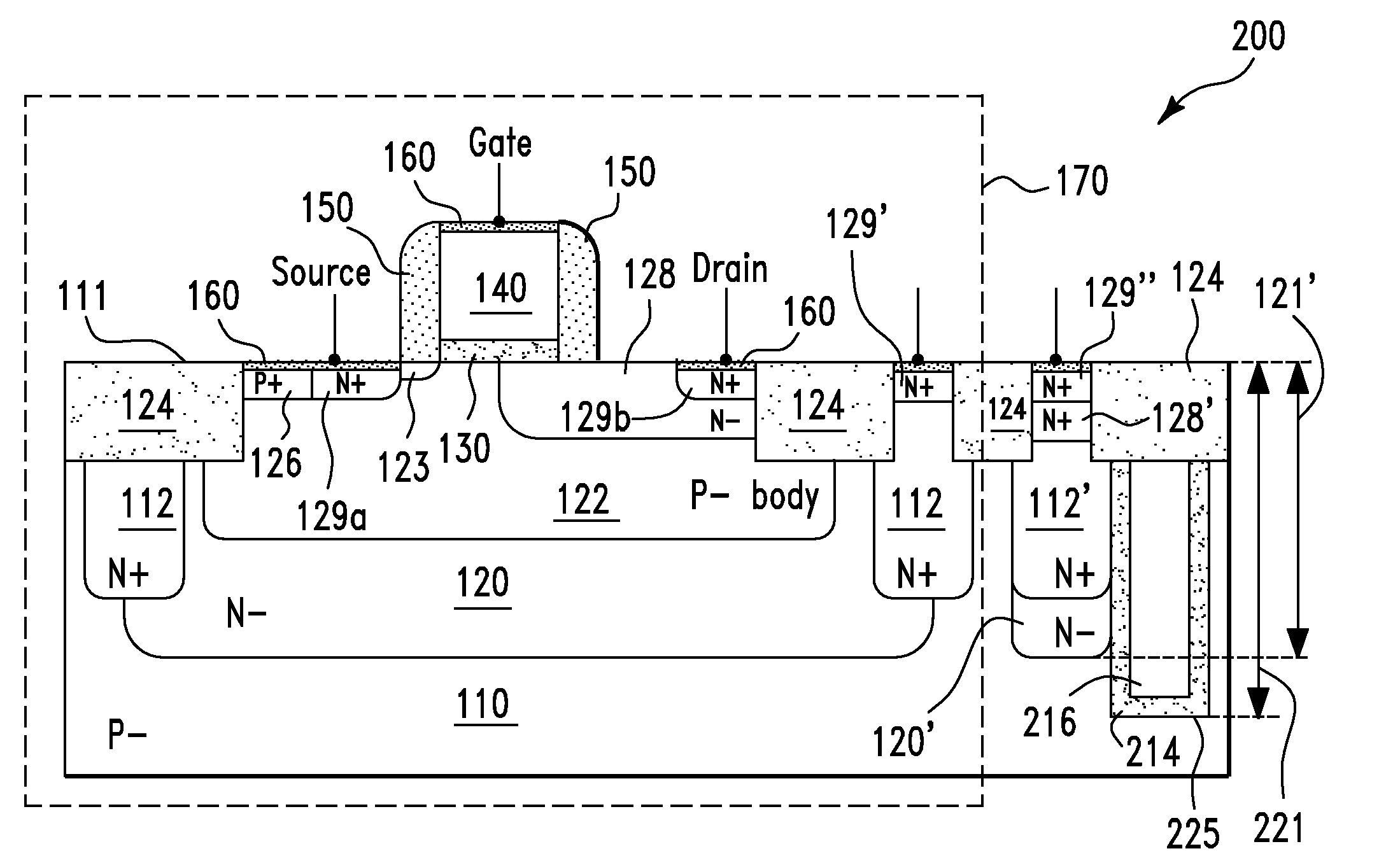
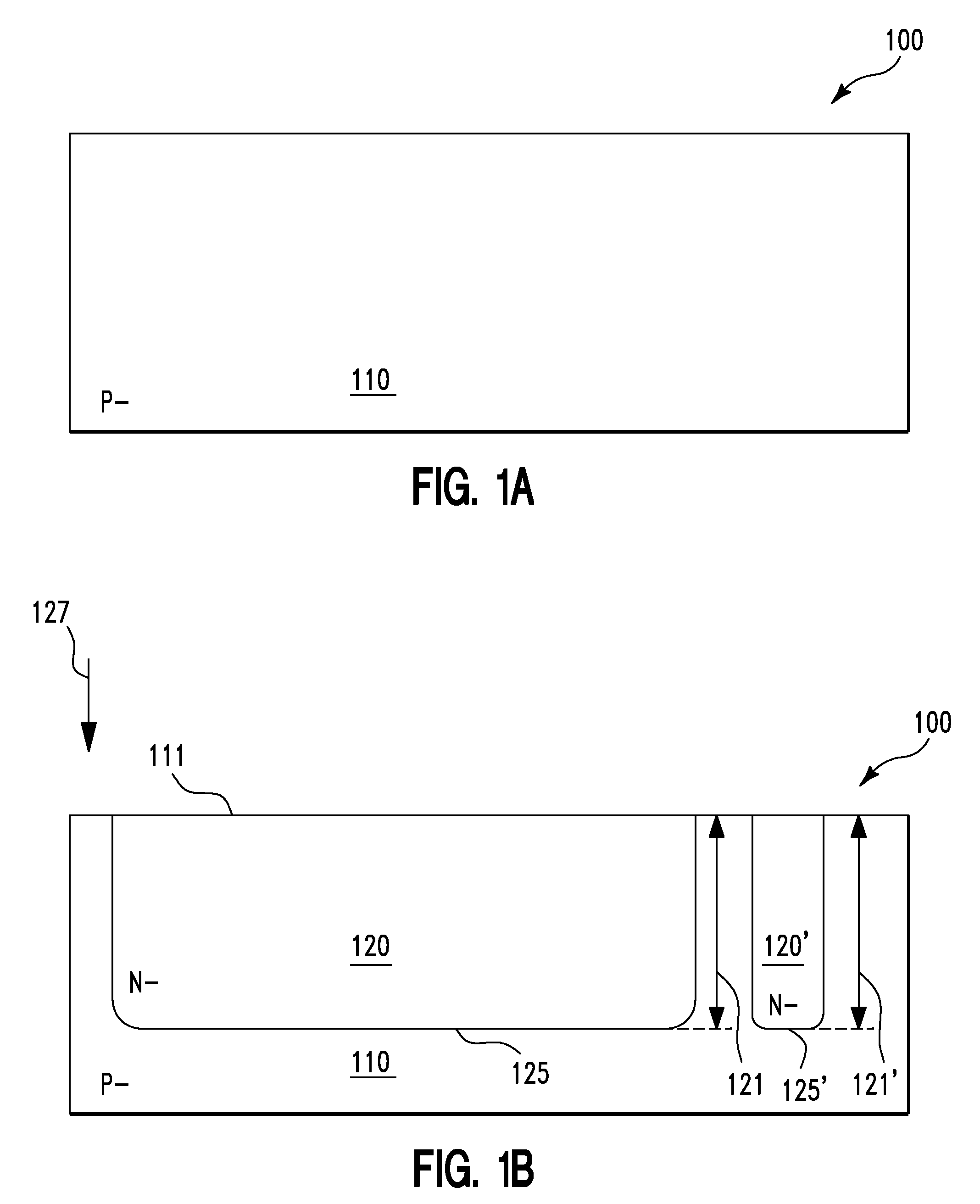
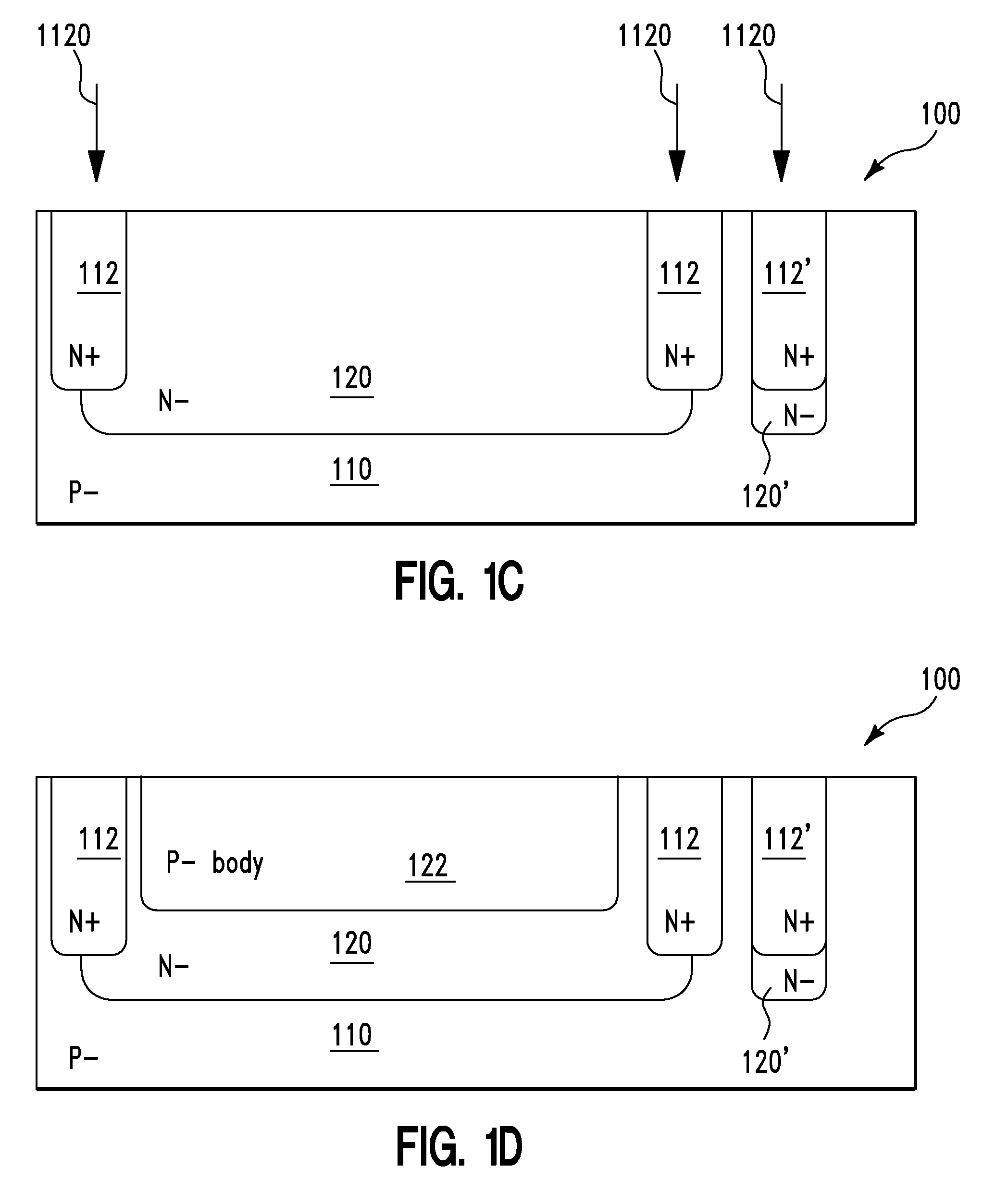
[0015]FIGS. 1A-1G′ show cross-section views used to illustrate a fabrication process of a semiconductor structure 100, in accordance with embodiments of the present invention. More specifically, with reference to FIG. 1A, the fabrication process of the semiconductor structure 100 starts with a P− substrate 110. The P− substrate 110 comprises silicon doped with p-type dopants (e.g., boron atoms). The P− substrate 110 can be formed by ion implanting p-type dopants into the semiconductor substrate 110 resulting in the P− substrate 110.

[0016]Next, with reference to FIG. 1B, in one embodiment, an N− region 120 and an N− region 120′ are formed in the P− substrate 110. The N− regions 120 and 120′ can be formed by (i) forming a photoresist layer (not shown) on top of the structure 100 of FIG. 1A, (ii) patterning the photoresist layer, and (iii) ion implanting n-type dopants into the P− substrate 110 with the patterned photoresist layer as a blocking mask resulting in the N− regions 120 and ...


PUM


Abstract

A semiconductor structure and a method for forming the same. The method includes providing a semiconductor structure. The semiconductor structure includes a semiconductor substrate. The method further includes simultaneously forming a first doped transistor region of a first transistor and a first doped guard-ring region of a guard ring on the semiconductor substrate. The first doped transistor region and the first doped guard-ring region comprise dopants of a first doping polarity. The method further includes simultaneously forming a second doped transistor region of the first transistor and a second doped guard-ring region of the guard ring on the semiconductor substrate. The second doped transistor region and the second doped guard-ring region comprise dopants of the first doping polarity. The second doped guard-ring region is in direct physical contact with the first doped guard-ring region. The guard ring forms a closed loop around the first and second doped transistor regions.

Description

FIELD OF THE INVENTION[0001]The present invention relates generally to guard ring structures and more particularly to guard ring structures in smart power technology using LDMOS (lateral double-diffused metal oxide semiconductor) device fabrication.BACKGROUND OF THE INVENTION[0002]Today, in smart power technology, high voltage CMOS (HVCMOS) and low voltage CMOS (LVCMOS) exist on a common wafer. Low voltage CMOS technology operates in the 1V to 5V power levels. HVCMOS technology operates between 20V to 120V power levels.[0003]In high voltage CMOS (HVCMOS) technology, a concern is the interaction between the LDMOS transistors and the adjacent low voltage CMOS circuitry. In HVCMOS, inductive “load dumps” initiate injection of carriers into the chip substrate. As a result of the physical size of the HVCMOS and LDMOS devices, as well as the magnitude of the current injection, it is critical not to disturb the other chip functions on the smart power chips.[0004]In addition, CMOS latchup i...

Claims


Application Information

Patent Timeline
IPC IPC(8): H01L27/06H01L21/8234
CPCH01L29/0619H01L29/0692H01L29/7835H01L29/1087H01L29/66659H01L29/1083
Inventor VOLDMAN, STEVEN HOWARD
Owner GLOBALFOUNDRIES INC
Why Eureka
Try Eureka