Method for Packaging Semiconductor Dies Having Through-Silicon Vias

a technology of silicon vias and semiconductor dies, applied in the field of integrated circuits, can solve the problems of high cost of polishing process, high cost of copper polishing process, and inability to meet the requirements of the application

Inactive Publication Date: 2009-01-22
TAIWAN SEMICON MFG CO LTD
View PDF9 Cites 46 Cited by
  • Summary
  • Abstract
  • Description
  • Claims
  • Application Information

AI Technical Summary

Problems solved by technology

This causes reliability issues.
Due to the tilting of die 10, some portion of the wire bonds, for example, wire 22, may not be fully covered by molding compound 20, and hence is subject to mechanical damage.
Further, the process for polishing copper is more costly than polishing silicon due to contamination issues.
Therefore, polishing back TSVs is a undesirable solution.

Method used


Image

  • Method for Packaging Semiconductor Dies Having Through-Silicon Vias
  • Method for Packaging Semiconductor Dies Having Through-Silicon Vias
  • Method for Packaging Semiconductor Dies Having Through-Silicon Vias

Examples


Embodiment Construction

[0015]The making and using of the presently preferred embodiments are discussed in detail below. It should be appreciated, however, that the present invention provides many applicable inventive concepts that can be embodied in a wide variety of specific contexts. The specific embodiments discussed are merely illustrative of specific ways to make and use the invention, and do not limit the scope of the invention.

[0016]A novel packaging structure and the methods for forming the same are provided. The intermediate stages of manufacturing embodiments of the present invention are illustrated. Throughout the various views and illustrative embodiments of the present invention, like reference numbers are used to designate like elements.

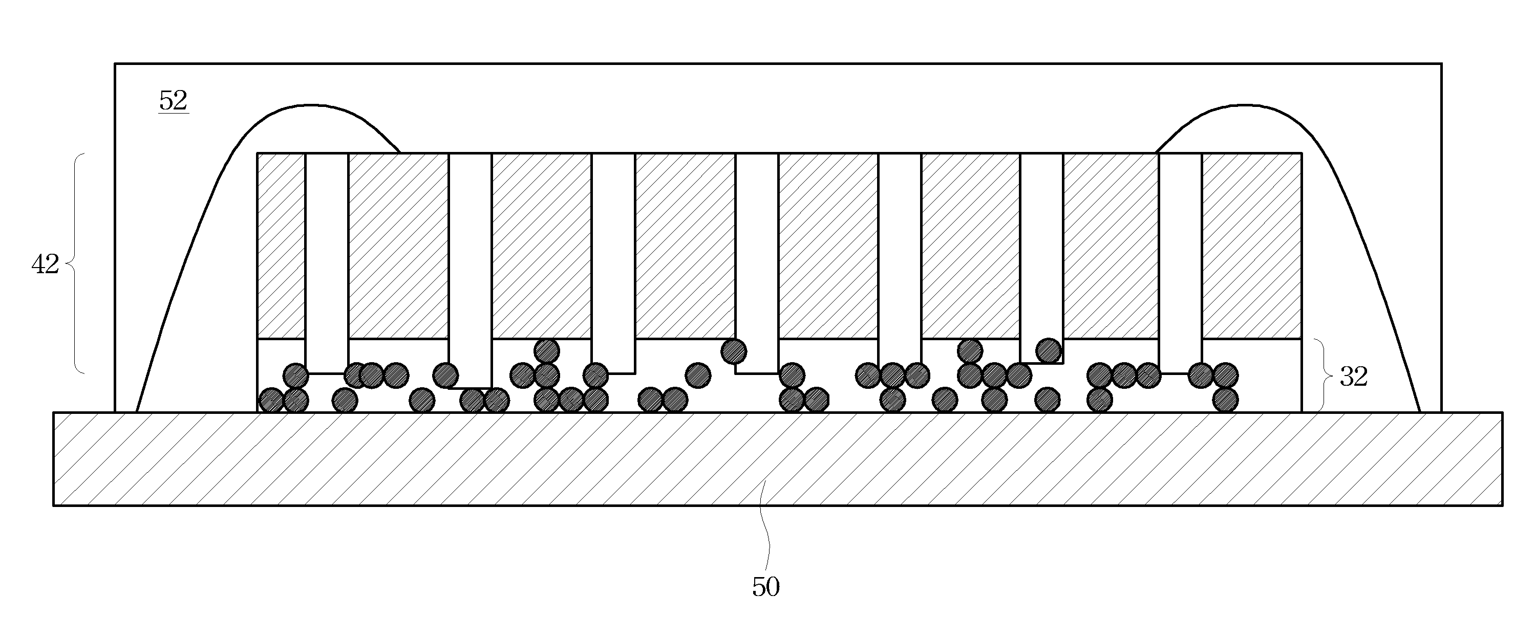
[0017]FIG. 4A illustrates integrated wafer-mount tape 30, which includes anisotropic conducting film (ACF) 32 and ultra-violet (UV) wafer-mount tape 34. As is known in the art, ACF 32 includes a plurality of conductive particles 36 insulated from each other b...


PUM

PropertyMeasurementUnit
thicknessaaaaaaaaaa
thicknessaaaaaaaaaa
temperatureaaaaaaaaaa

Abstract

An integrated circuit structure is provided. The integrated circuit structure includes a die and an anisotropic conducing film (ACF) adjoining the back surface of the die. The die includes a front surface; a back surface on an opposite side of the die than the front surface; and a through-silicon via (TSV) exposed through the back surface of the die.

Description

TECHNICAL FIELD[0001]This invention relates generally to integrated circuits, and more particularly to the packaging of semiconductor dies, and even more particularly to the packaging of semiconductor dies having through-silicon vias.BACKGROUND[0002]Through-silicon vias (TSV), also commonly referred to as through-wafer vias (TWV), are widely used in integrated circuits. TSVs can be used for stacking dies. In stacked dies including a first die stacked on a second die, electrical connections may be made from the first die to the top surface of the second die through TSVs in the first die. TSVs are also commonly used for providing a quick and low-resistive path from a front surface of a die to its back surface.[0003]FIGS. 1 through 3 illustrate cross-sectional views of intermediate stages in a conventional process for forming TSVs in a die and grounding the die through the TSVs. Referring to FIG. 1, TSVs 12 are formed in die 10, and extend from substantially the front surface (the top ...

Claims


Application Information

Patent Timeline
Patent Type & Authority Applications(United States)
IPC IPC(8): H01L21/00B32B7/12H01L23/04
CPCH01L21/6836H01L23/481H01L24/13H01L24/16H01L24/27H01L24/29H01L24/32H01L24/48H01L24/73H01L24/83H01L24/94H01L2221/68327H01L2224/13009H01L2224/13099H01L2224/16225H01L2224/32225H01L2224/48091H01L2224/48221H01L2224/48227H01L2224/83191H01L2224/838H01L2224/94H01L2924/01015H01L2924/01027H01L2924/01029H01L2924/01047H01L2924/01079H01L2924/01082H01L2924/0781H01L2924/14H01L2924/01005H01L2924/01006H01L2924/01019H01L2924/01033H01L2924/0665H01L2924/00013H01L2224/2939H01L2224/29455H01L2224/2929H01L2224/29444H01L2924/10253H01L23/52H01L2224/27436H01L2224/29082H01L2224/29499H01L2224/83851H01L2224/27003Y10T428/26Y10T428/28H01L2224/03H01L2924/00014H01L2924/00H01L2224/29299H01L2224/29099H01L2224/29199H01L2224/451H01L2924/15788H01L2924/181H01L2224/05573H01L2224/13025H01L2224/73257H01L2224/05599H01L2924/00012H01L2224/45099H01L2224/45015H01L2924/207
Inventor SU, CHAO-YUAN
Owner TAIWAN SEMICON MFG CO LTD
Why Eureka
Try Eureka