Piezoelectric oscillator and transmitter

a technology of piezoelectric oscillator and transmitter, which is applied in the direction of oscillator, transmission, electrical apparatus, etc., can solve the problems of increasing mounting space, difficult downsizing of piezoelectric oscillator or the transmitter using piezoelectric oscillator, and large values, so as to improve the space efficiency inside the package, reduce the size of the package, and reduce the size of the piezoelectric oscillator

Inactive Publication Date: 2009-01-22
SEIKO EPSON CORP
View PDF3 Cites 28 Cited by
  • Summary
  • Abstract
  • Description
  • Claims
  • Application Information

AI Technical Summary

Benefits of technology

[0009]An advantage of the invention is to provide a piezoelectric oscillator including a matching circuit and a transmitter equipped with the piezoelectric oscillator.
[0010]A piezoelectric oscillator according to a first aspect of the invention includes: a piezoelectric resonator element having a piezoelectric substrate and an excitation electrode formed on a surface of the piezoelectric substrate; a semiconductor circuit element provided with an oscillation circuit for oscillating the piezoelectric resonator element, and having a first insulating film formed on a principal surface; a package for airtightly housing the semiconductor circuit element and the piezoelectric resonator element; and a protruding section having at least of a thin film circuit component formed on the first insulating film and connected to the oscillation circuit, and a second insulating film formed on the first insulating film and covering the thin film circuit component. In the oscillator, the piezoelectric resonator element is fixed to an upper surface of the protruding section.
[0011]According to this configuration, in the piezoelectric oscillator, since the semiconductor circuit element and the piezoelectric resonator element can be disposed in an overlapping manner in plan view by fixing the piezoelectric resonator element on the protruding section of the principal surface of the semiconductor circuit element provided with the oscillation circuit, the space efficiency inside the package is improved, thus downsizing of the package becomes possible. Therefore, downsizing of the piezoelectric oscillator becomes possible.
[0012]Further, in the piezoelectric oscillator, since the piezoelectric resonator element is fixed on the protruding section on the principal surface of the semiconductor circuit element, it is possible to provide the distance equivalent to the thickness of the protruding section between the principal surface of the semiconductor circuit element and piezoelectric resonator element. Thus, in the piezoelectric oscillator, since the collision between the semiconductor circuit element and the piezoelectric resonator element in response to, for example, the dropping impact becomes hard to occur. As a result, the impact resistance can be improved.
[0013]In addition, in the piezoelectric oscillator, since the thin film circuit component to be connected to the oscillation circuit is formed on the first insulating film, the circuit component with such a large circuit parameter as to cause difficulty in forming the circuit component in the semiconductor circuit element can be formed on the semiconductor circuit element. Thus, in the piezoelectric oscillator, since there is no need for mounting an external circuit component in the separate space inside the package, downsizing of the package becomes possible. Therefore, downsizing of the piezoelectric oscillator becomes possible.
[0014]In the piezoelectric oscillator, the piezoelectric resonator element is preferably fixed to the upper surface of the protruding section so that the piezoelectric resonator element is within a contour of the semiconductor circuit element in plan view.

Problems solved by technology

As the circuit parameters such as resistances, capacitances, or inductances required to the circuit components such as resistor elements, capacitor elements, or inductive elements used in such cases, large values, which are difficult to form by integrating them in an IC chip using the CMOS process, are required.
Therefore, since it is necessary to use the resistor elements, the capacitor elements, or the inductive elements formed as relatively large chip components, there is caused a problem that increase in mounting space is resulted, and thus downsizing of the piezoelectric oscillator or the transmitter using the piezoelectric oscillator becomes difficult.
Further, in the case in which downsizing of the piezoelectric oscillator or the transmitter using the piezoelectric oscillator is given greater importance, and the matching circuit is not incorporated therein, the matching circuit needs to be provided to the mounting circuit board of the counter part on which the piezoelectric oscillator or the transmitter using the piezoelectric oscillator is mounted, and there is caused a problem that the advantage of downsizing of the entire communication device is reduced by half.
In addition, in the piezoelectric oscillator, since the thin film circuit component to be connected to the oscillation circuit is formed on the first insulating film, the circuit component with such a large circuit parameter as to cause difficulty in forming the circuit component in the semiconductor circuit element can be formed on the semiconductor circuit element.

Method used


Image

  • Piezoelectric oscillator and transmitter
  • Piezoelectric oscillator and transmitter
  • Piezoelectric oscillator and transmitter

Examples


first embodiment

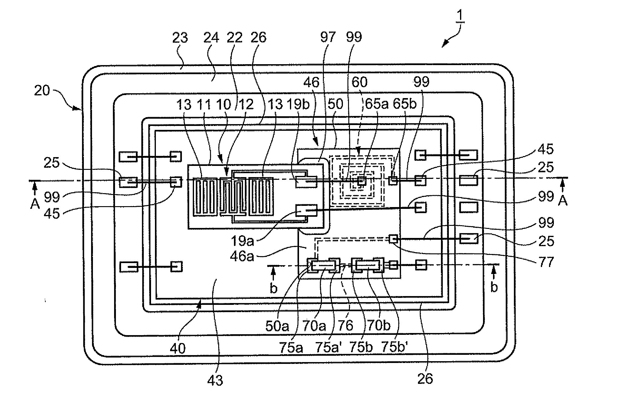
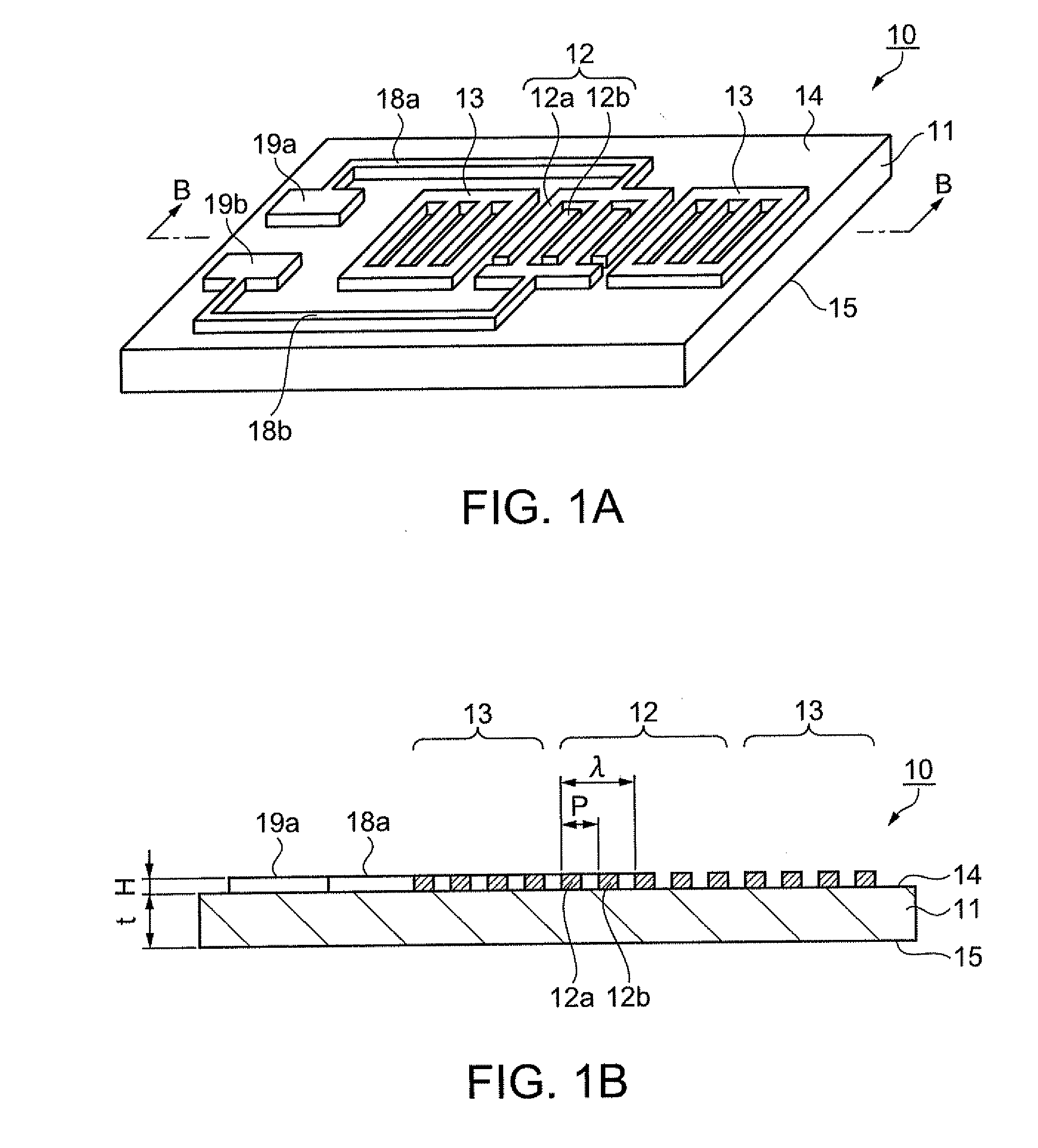
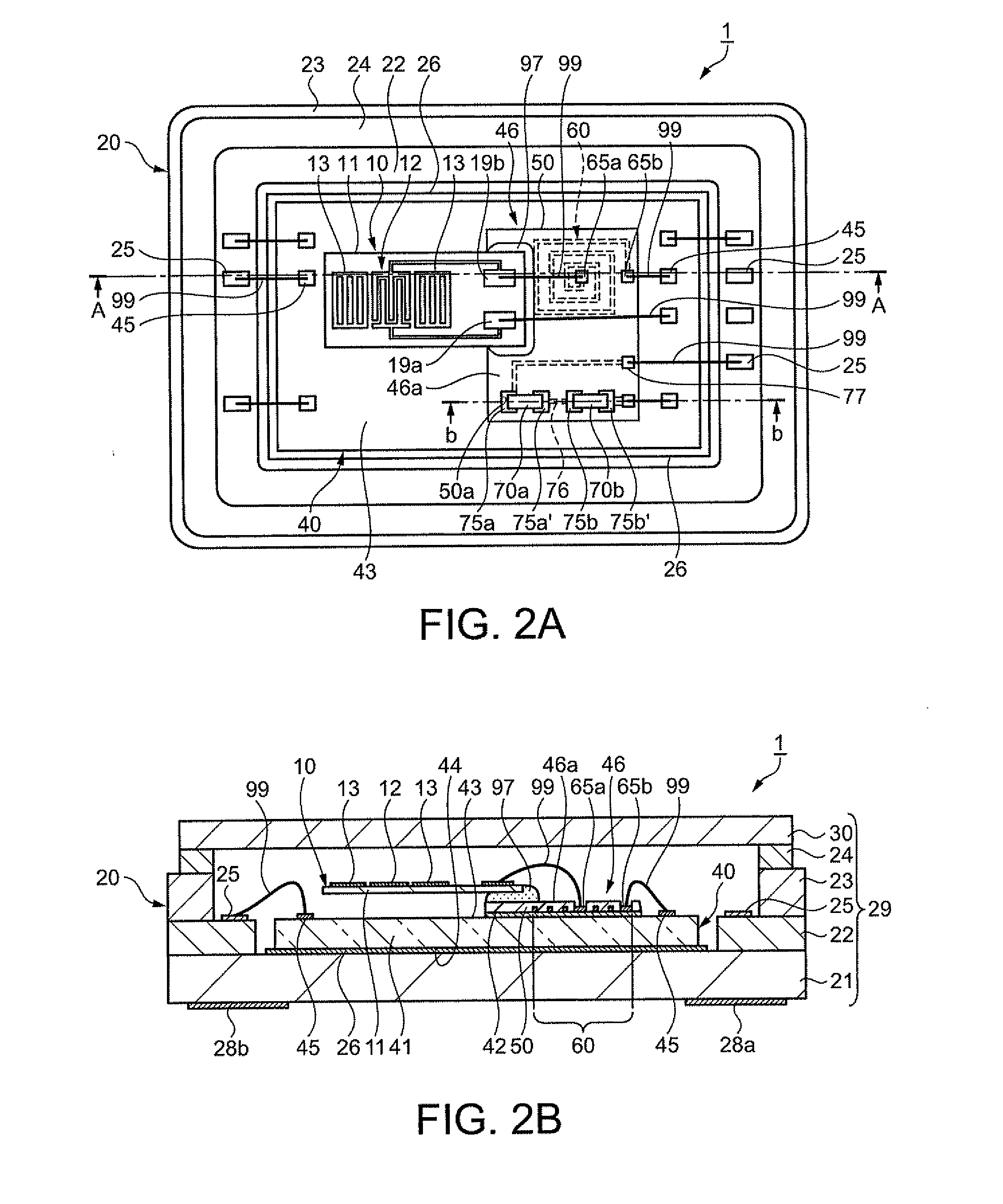
[0044]FIGS. 1A and 1B are diagrams for explaining the SAW resonator as the piezoelectric resonator element mounted on the SAW oscillator according to the present embodiment, wherein FIG. 1A is a perspective view, and FIG. 1B is a cross-sectional view along the B-B line shown in FIG. 1A. Further, FIGS. 2A and 2B are diagrams for explaining the SAW oscillator according to the present embodiment, wherein FIG. 2A is a plan view, and FIG. 2B is a cross-sectional view along the A-A line shown in FIG. 2A. It should be noted that in FIG. 2A, a metal lid as a lid member disposed on the upper part of the SAW oscillator is omitted from illustration for the sake of convenience of explanation of the internal configuration of the SAW oscillator. Further, FIG. 3 is a cross-sectional view along the b-b line shown in FIG. 2A, enlarging the part of the SAW oscillator according the present embodiment, on which circuit component chips are mounted, for explaining the part.

[0045]SAW Resonator

[0046]Firstl...

first modified example

[0096]Here, a first modified example of the first embodiment of the invention will be explained with reference to the drawing. FIG. 4 is a cross-sectional view of an SAW oscillator according to the first modified example of the first embodiment. It should be noted that the common sections to the first embodiment are denoted with the same reference numerals, the explanations therefor will be omitted, and different sections will mainly be explained.

[0097]As shown in FIG. 4, the SAW oscillator 101 according to the first modified example of the first embodiment has a spacing member 80 interposed between the one principal surface 43 of the IC chip 40 and the first insulating film 42. As the spacing member 80, a silicon substrate or the like is used. The spacing member 80 is fixed to the one principal surface 43 of the IC chip 40 with an adhesive not shown in the drawing.

[0098]It should be noted that it is preferable that the spacing member 80 is fixed to the IC chip 40 after the first in...

second modified example

[0100]Then, a second modified example of the first embodiment of the invention will be explained with reference to the drawing.

[0101]FIG. 5 is a cross-sectional view of an SAW oscillator according to the second modified example of the first embodiment. It should be noted that the common sections to the first embodiment are denoted with the same reference numerals, the explanations therefor will be omitted, and different sections will mainly be explained.

[0102]As shown in FIG. 5, the SAW oscillator 102 according to the second modified example of the first embodiment has the first insulating film 422 formed on the entire one principal surface 43 of the IC chip 402.

[0103]In such a case, the extended coil 602 as the inductive element, which is a thin film circuit component connected to the oscillation circuit described above, is formed on the first insulating film 422. Further, the protruding section 462 is formed on the extended coil 602 and the first insulating film 422 so as to have ...


PUM


Abstract

A piezoelectric oscillator includes: a piezoelectric resonator element having a piezoelectric substrate and an excitation electrode formed on a surface of the piezoelectric substrate; a semiconductor circuit element provided with an oscillation circuit for oscillating the piezoelectric resonator element and having a first insulating film formed on a principal surface; a package for airtightly housing the semiconductor circuit element and the piezoelectric resonator element; and a protruding section having at least of a thin film circuit component formed on the first insulating film and connected to the oscillation circuit; and a second insulating film formed on the first insulating film and covering the thin film circuit component. In the oscillator, the piezoelectric resonator element is fixed to an upper surface of the protruding section,

Description

BACKGROUND[0001]1. Technical Field[0002]The present invention relates to a piezoelectric oscillator and a transmitter equipped with the piezoelectric oscillator.[0003]2. Related Art[0004]In recent years, in order for coping with increase in communication speed associated with rapid development in the information-communication technology and the network technology, oscillators used for communication devices are required to be high-frequency devices and to have high stability. Surface acoustic wave (hereinafter also referred to as “SAW”) oscillators, each of which is composed of a SAW resonator as a piezoelectric resonator element using a surface acoustic wave and a semiconductor circuit element (hereinafter referred to as “an IC chip”) having an oscillating circuit for driving the SAW resonator as an integrated circuit, are widely used as the oscillators suitable to have a high-frequency property, and transmitters and so on equipped with the SAW oscillators are also used widely. Furt...

Claims


Application Information

Patent Timeline
Patent Type & Authority Applications(United States)
IPC IPC(8): H04B1/04H03B5/30
CPCH03B1/02H03B5/36
Inventor NISHIO, SHINJI
Owner SEIKO EPSON CORP
Why Eureka
Try Eureka