

Nitride light emitting device and manufacturing method thereof
- Summary
- Abstract
- Description
- Claims
- Application Information
AI Technical Summary
Benefits of technology
Problems solved by technology
Method used
Image

Examples
first embodiment
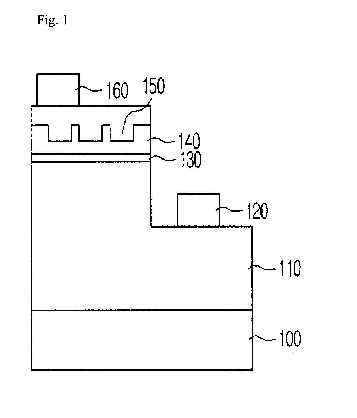
[0021]FIG. 1 is a cross-sectional view of a nitride light emitting device according to the first embodiment of the present invention.
[0022]As illustrated in FIG. 1, the nitride light emitting device according to the embodiment of the present invention includes a substrate 100, a first conduction type cladding layer 110 formed on the substrate 100, an active layer 130 formed on the first conduction type cladding layer 110, and a second conduction type cladding layer 140 formed on the active layer 130.
[0023]The nitride light emitting device according to the embodiment of the present invention may further include a first electrode 120 formed on the first conduction type cladding layer 110, and a second electrode 160 formed on the second conduction type cladding layer 140. The first electrode 120 can be an n-type electrode, and the second electrode 160 can be a p-type electrode. Also, the first electrode 120 can be a p-type electrode, and the second electrode 160 can be an n-type electr...
second embodiment
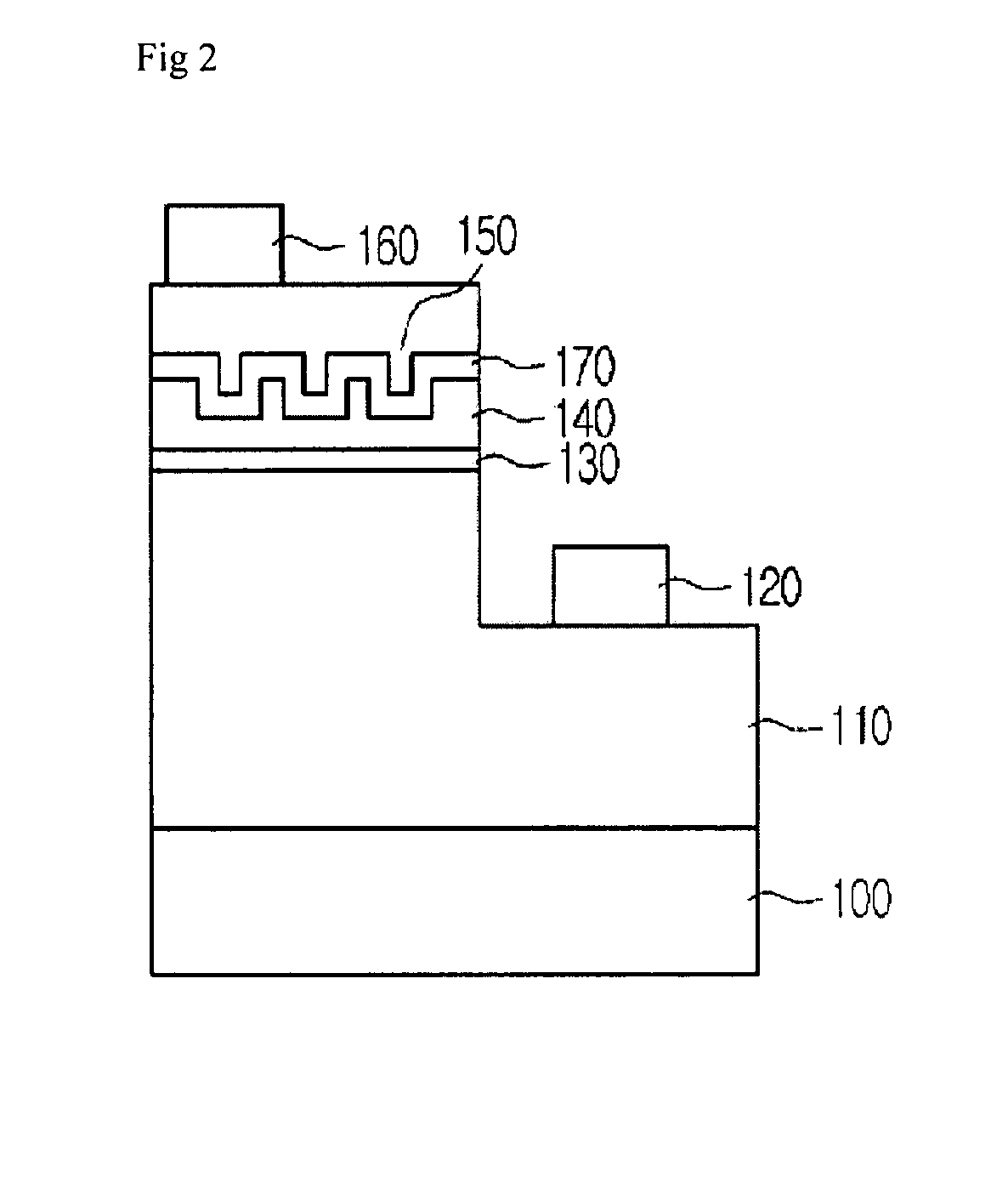
[0038]FIG. 2 is a cross-sectional view of a nitride light emitting device according to the second embodiment of the present invention.
[0039]The second embodiment of the present invention is an example of a nitride light emitting device having an npn junction structure.
[0040]As illustrated in FIG. 2, the nitride light emitting device according to the second embodiment of the present invention includes a substrate 100, a first conduction type cladding layer 110, a first electrode 120, an active layer 130, a second conduction type cladding layer 140, a third conduction type cladding layer 170, a transparent electrode 150, and a second electrode 160.
[0041]The nitride light emitting device according to the second embodiment of the present invention is different from that of the first embodiment in that a third conduction type cladding layer 170 is further formed between the second conduction type cladding layer 140 and the transparent layer 150.
[0042]The third conduction type cladding la...
third embodiment
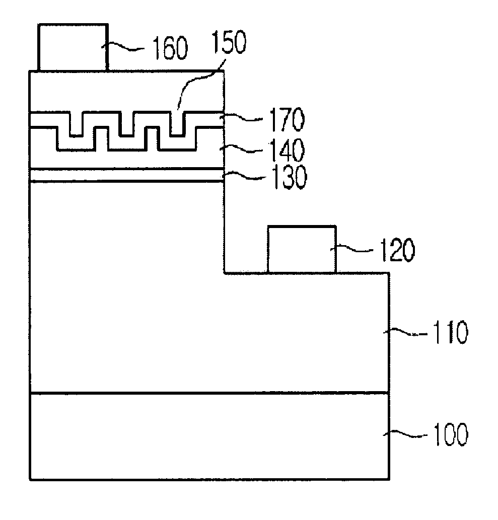
[0048]FIG. 3 is a cross-sectional view of a nitride light emitting device according to the third embodiment of the present invention.
[0049]The third embodiment of the present invention is an example of a nitride light emitting device having an npn junction structure.
[0050]As illustrated in FIG. 3, the nitride light emitting device according to the third embodiment of the present invention may include a substrate 100, a first conduction type cladding layer 110, a first electrode 120, an active layer 130, a second conduction type cladding layer 140, a third conduction type cladding layer 170, a transparent electrode 150, and a second electrode 160.
[0051]The nitride light emitting device according to the third embodiment of the present invention is different from that of the second embodiment in that a top surface of the third conduction type cladding layer 170 is formed flat.
PUM
 Abstract
Description
Claims
Application Information