Methods for forming electrodes in phase change memory devices

a phase change memory and electrode technology, applied in the field of forming electrodes in phase change memory devices, can solve the problems of reducing the contact area of one or more electrodes, limiting the goal of device miniaturization, and reducing the processing efficiency of devices, so as to reduce the structural irregularities of electrode materials, reduce the volume fraction of voids, and increase the uniformity and density of filling. effect of the density

Inactive Publication Date: 2009-01-29
OVONYX
View PDF9 Cites 40 Cited by
  • Summary
  • Abstract
  • Description
  • Claims
  • Application Information

AI Technical Summary

Benefits of technology

[0022]The methods for forming the electrode material include extrusion and reflow. The electrode formation methods are designed to selectively and conformally fill or occupy the opening with an electrode material. The methods reduce structural irregularities of the electrode material within the opening and promote more uniform and higher density filling of openings by reducing the volume fraction of voids and structural defects.

Problems solved by technology

One of the significant practical challenges that programmable resistance memory and switching devices face is to reduce the contact area of one or more electrodes contacting the active material.
Lithography is a patterning process in the formation of semiconductor devices that is commonly used to define small-scale features and often sets a limit on the goal of device miniaturization.
As the feature size of devices is minimized, however, processing of the devices becomes more difficult.
Small scale features become more difficult to define as the lithographic limit of resolution is reached and features that are defined become more difficult to process.
As the dimension or length scale of an opening decreases upon miniaturization, it becomes increasingly difficult to fill the opening with another material without compromising performance or durability.
Techniques such as physical vapor deposition (PVD) or sputtering fail to provide dense or complete filling of openings when the dimensions of the opening are reduced below a critical size.
Instead of providing a dense, uniform filling, these techniques increasingly incompletely fill openings as the feature size of the opening decreases.
As the feature size decreases, there is a tendency for the packing density of the material formed in the opening to vary in the depth or lateral dimensions of the opening and as a result, the layer deposited within the opening may include voids, vacancies, gaps, pores, keyholes, or other non-uniform regions.
Deep, narrow channels, for example, are more difficult to fill uniformly than channels that are shallow and wide.
With deep, narrow features, sputtering and other physical deposition techniques are oftentimes unable to deliver sufficient material to the bottom of the feature.
Lack of structural uniformity in the filling of openings compromises performance because: (1) variations in device characteristics occur across an array due to differences in the degree or nature of filling non-uniformities from device-to-device and (2) less than optimal performance is achieved for each device due to the defective nature of the material within the opening.
Conformality of deposition is another processing difficulty that becomes exacerbated as feature size decreases.
In addition to difficulties with achieving uniform filling, openings also present complications for achieving conformal deposition that become more pronounced as size of the opening decreases.
Achieving conformality over discontinuous features becomes increasingly difficult as the feature size of the opening decreases or the aspect ratio of the opening increases.
The imperfections detract from device performance.

Method used


Image

  • Methods for forming electrodes in phase change memory devices
  • Methods for forming electrodes in phase change memory devices
  • Methods for forming electrodes in phase change memory devices

Examples


Embodiment Construction

[0037]The making and using of the presently preferred embodiments are discussed in detail below. It should be appreciated, however, that the present invention provides many applicable inventive concepts that can be embodied in a wide variety of specific contexts. The specific embodiments discussed are merely illustrative of specific ways to make and use the invention, and do not limit the scope of the invention.

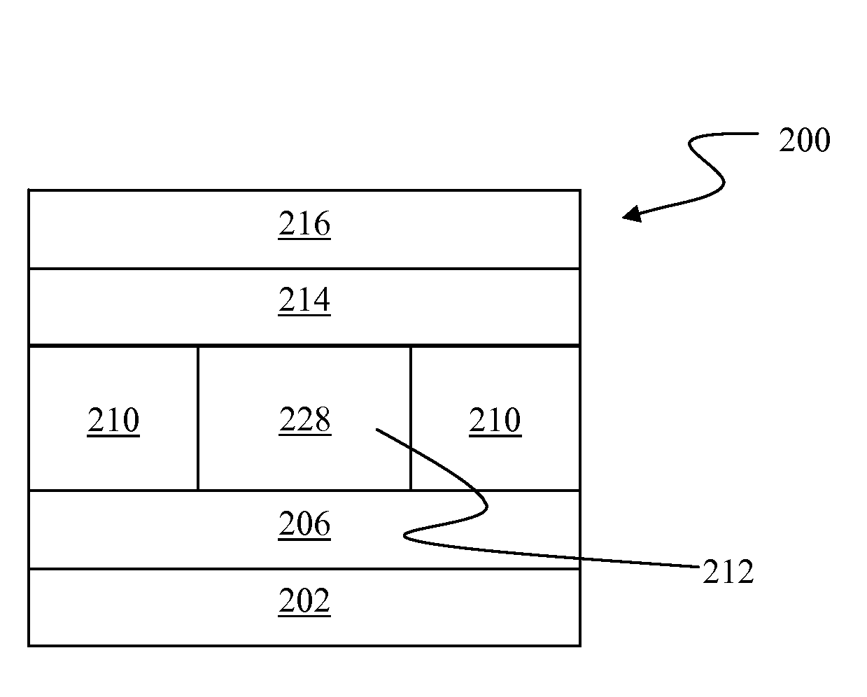
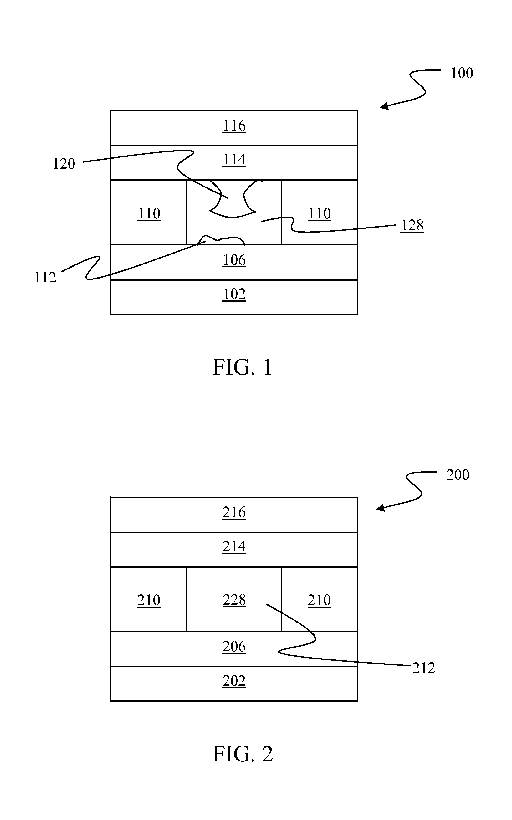
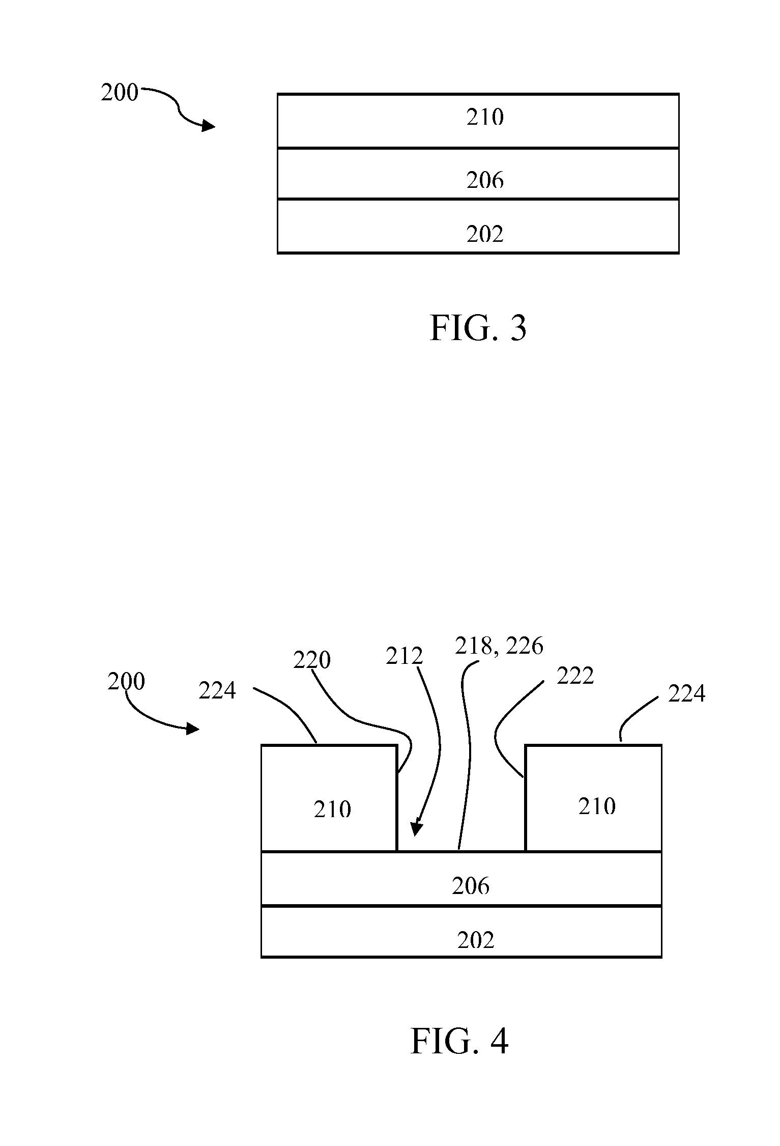
[0038]The instant invention relates generally to electronic devices that include two or more electrodes in contact or electrical communication with an active material. As used herein, active material refers generally to an electrically stimulable material such as a programmable resistance material used for memory, programmable logic, or other applications; other memory material; or electrical switching material. A programmable resistance material is a material having two or more states that are distinguishable on the basis of electrical resistance. The two or more states may ...


PUM

PropertyMeasurementUnit
aspect ratioaaaaaaaaaa
feature sizeaaaaaaaaaa

Abstract

A method for forming electrode materials uniformly within openings having small dimensions, including sublithographic dimensions, or high aspect ratios. The method includes the steps of providing an insulator layer having an opening formed therein, forming a non-conformal conductive or semiresistive material over and within the opening, and mobilizing the conductive material to densify it within the opening. The method reduces the concentration of voids or defects in the conductive or semiresistive material relative to the as-deposited state. The mobilizing step may be accomplished by extrusion or thermal reflow and causes voids or defects to coalesce, collapse, percolate, or otherwise be removed from the as-deposited conductive or semiresistive material.

Description

CROSS-REFERENCE TO RELATED APPLICATIONS[0001]This application is a continuation in part of U.S. patent application Ser. No. 11 / 880,587, entitled “Liquid Phase Deposition of Contacts in Programmable Resistance and Switching Devices” and filed on Jul. 23, 2007; and a continuation in part of U.S. patent application Ser. No. 12 / 075,222, entitled “Pressure Extrusion Method for Filling Features in the Fabrication of Electronic Devices and filed on Mar. 10, 2008; and a continuation in part of U.S. patent application Ser. No. 12 / 075,180, entitled “Temperature and Pressure Control Methods to Fill Features within Programmable Resistance and Switching Devices” and filed on Mar. 10, 2008; all of which disclosures are incorporated in their entirety herein.FIELD OF INVENTION[0002]This invention relates generally to programmable resistance and switching devices having one or more electrodes. More particularly, this invention relates to methods for forming electrodes for programmable resistance and...

Claims


Application Information

Patent Timeline
Patent Type & Authority Applications(United States)
IPC IPC(8): B05D5/12
CPCH01L45/06H01L45/1233H01L45/1683H01L45/144H01L45/16H01L45/126H10N70/8413H10N70/231H10N70/066H10N70/011H10N70/8828H10N70/826H10N70/8825
Inventor LOWREY, TYLER
Owner OVONYX
Why Eureka
Try Eureka