

Photosensitive Resin Composition, Photosensitive Element, Method for Forming Resist Pattern and Method for Producing Printed Wiring Board
a technology of photosensitive resin and resist pattern, which is applied in the direction of photosensitive materials, instruments, photomechanical equipment, etc., can solve the problems of unsatisfactory sensitivity and resolution of existing photosensitive resin compositions, and achieve high productivities, satisfactory sensitivity, and high density resist pattern
Active Publication Date: 2009-01-29
RESONAC CORP
View PDF7 Cites 7 Cited by
- Summary
- Abstract
- Description
- Claims
- Application Information
AI Technical Summary
Benefits of technology
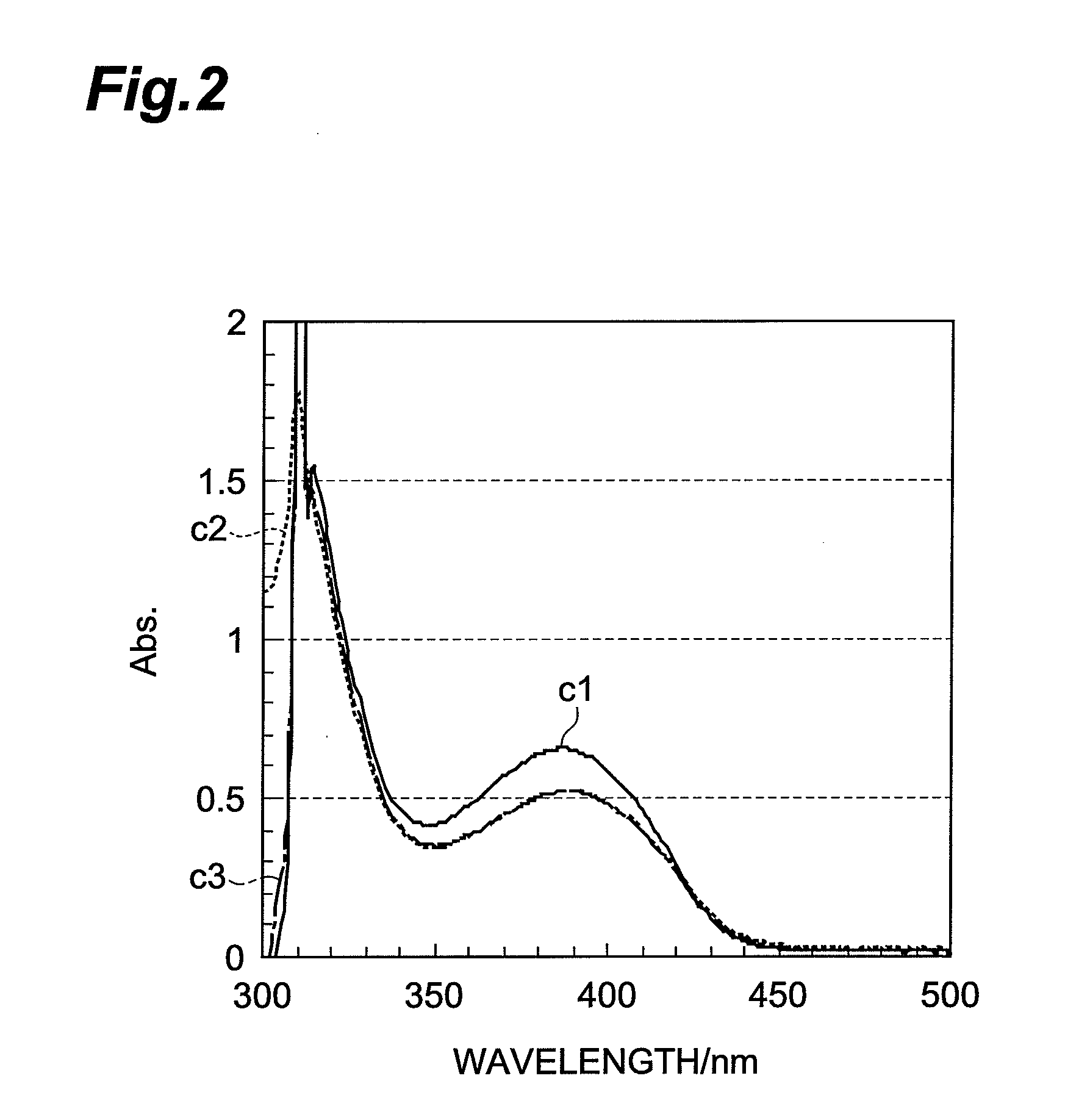
The present invention provides a photosensitive resin composition that can be used for high-density resist pattern formation by direct imaging exposure with a satisfactory sensitivity and resolution. The composition includes a binder polymer, a photopolymerizable compound, and a compound represented by general formula (1). The use of a specific photopolymerization initiator, namely a pyrazoline derivative, in combination with other components in the composition, results in an improved sensitivity and resolution. The photosensitive resin composition can be used to form resist patterns with high-density and good adhesiveness for printed wiring boards. The composition has a wavelength of maximum absorption in the range from at least 370 nm to less than 440 nm, which makes it suitable for direct imaging exposure using light having these specific wavelengths.
Problems solved by technology
However, the existing photosensitive resin compositions are still unsatisfactory with regard to sensitivity and resolution when employed for the formation of high-density resist patterns by direct imaging exposure.
Method used
View moreImage
Smart ImageViewing Examples

Examples
examples
[0103]The present invention is described in additional detail by the examples that follow, but the present invention is not limited to these examples.
Login to View More PUM
| Property | Measurement | Unit |
|---|---|---|
| wavelength range | aaaaa | aaaaa |
| wavelength range | aaaaa | aaaaa |
| wavelength | aaaaa | aaaaa |
Abstract
A photosensitive resin composition comprising: (A) a binder polymer; (B) a photopolymerizable compound that has an ethylenically unsaturated bond; and (C1) a compound represented by general formula (1) below,wherein, at least one R represents a C1-10 alkoxy group or a C1-12 alkyl group; the sum of a, b, and c is 1 to 6; and when the sum of a, b, and c is 2 to 6, each R may be the same as or different from one another.
Description
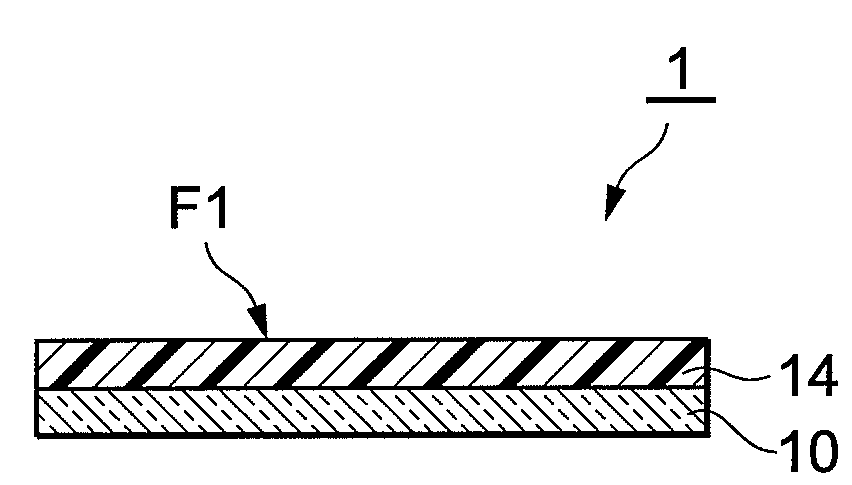
TECHNICAL FIELD[0001]The present invention relates to a photosensitive resin composition, a photosensitive element, a method for forming a resist pattern, and a method for producing printed wiring boards.BACKGROUND ART[0002]Microelectronic circuits, as encountered with, for example, wiring boards for plasma displays, wiring boards for liquid-crystal displays, large-scale integrated circuits, thin transistors, semiconductor packages, and so forth, are typically produced through a process known as photolithography that involves the formation of a resist pattern. In photolithography, a conductor pattern is formed on a substrate, for example, as follows. A photosensitive layer disposed on the substrate is first exposed to light, for example, ultraviolet radiation, through a mask film bearing a prescribed pattern. A resist pattern is then formed by development with a developing solution in which the exposed regions and unexposed regions have different solubilities. Then a conductor patte...
Claims
Login to View More Application Information
Patent Timeline
 Patent Type & AuthorityApplications(United States)
IPC IPC(8): G03F7/032G03F7/20
CPCC08F2/50G03F7/031Y10S430/146Y10S430/114Y10S430/106Y10S430/116Y10S430/121G03F7/0045G03F7/0047G03F7/027
InventorMIYASAKA, MASAHIROKUMAKI, TAKASHI
OwnerRESONAC CORP