Method of manufacturing semiconductor device

a manufacturing method and semiconductor technology, applied in the direction of printed circuit manufacturing, cross-talk/noise/interference reduction, printed circuit aspects, etc., can solve the problems of large silica content, difficult to roughen and the roughness cannot be controlled, so as to reduce the effect of roughening the surface of the sealing resin and reducing the cost of the semiconductor devi

Inactive Publication Date: 2009-01-29
SHINKO ELECTRIC IND CO LTD
View PDF4 Cites 17 Cited by
  • Summary
  • Abstract
  • Description
  • Claims
  • Application Information

AI Technical Summary

Benefits of technology

[0015]In consideration of the problems, therefore, it is an object of the invention to provide a method of manufacturing a semiconductor device capable of reducing a cost of the semiconductor device having a shielding function for blocking an electromagnetic wave.
[0021]According to the invention, the silica filler present on the surface of the sealing resin is dissolved in a hydrogen fluoride solution. Consequently, it is possible to roughen the surface of the sealing resin. By a plating method which is more inexpensive than the electromagnetic wave absorbing sheet, thus, a shield layer connected electrically to the ground terminal can be formed on the surface of the roughened sealing resin. Therefore, it is possible to reduce the cost of the semiconductor device.
[0022]According to the invention, it is possible to reduce a cost of a semiconductor device having a shielding function for blocking an electromagnetic wave.

Problems solved by technology

It is hard to roughen a surface of the sealing resin 107 containing the silica filler in a large amount through a conventional resin surface roughening treatment (a treatment carried out through permanganate etching, for example) (a silica content is large and a roughed shape cannot be controlled).
However, the electromagnetic wave absorbing sheet 108 is expensive.
For this reason, there is a problem in that the use of the electromagnetic wave absorbing sheet 108 causes a cost of the semiconductor device 100 to be increased.

Method used


Image

  • Method of manufacturing semiconductor device
  • Method of manufacturing semiconductor device
  • Method of manufacturing semiconductor device

Examples


first embodiment

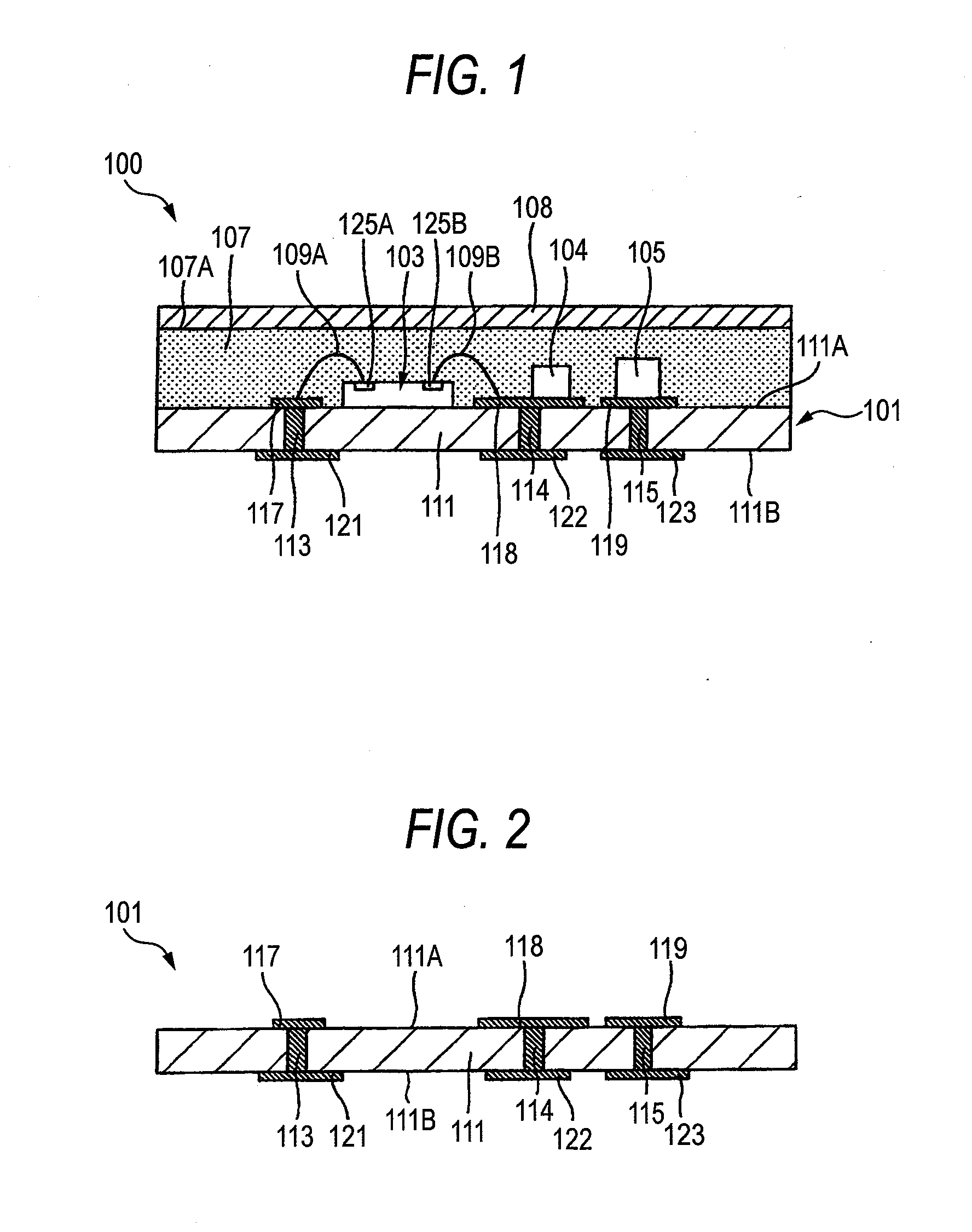
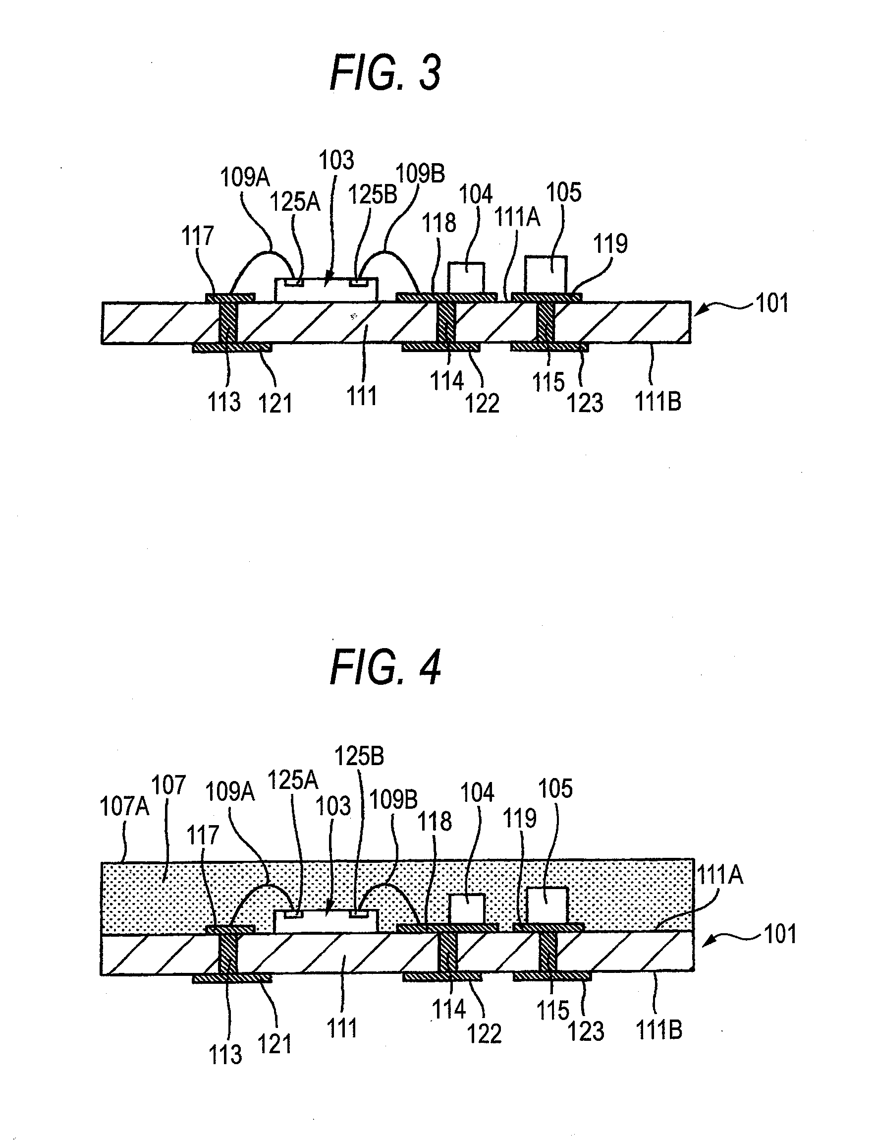
[0041]FIG. 6 is a sectional view showing a semiconductor device according to a first embodiment of the invention.

[0042]With reference to FIG. 6, a semiconductor device 10 according to the first embodiment comprises a wiring board 11, a semiconductor chip 12 and passive components 14 and 15 which are electronic components, metal wires 16 and 17, a sealing resin 19 and a shield layer 21.

[0043]The wiring board 11 has a board body 23, through vias 25 to 27, wiring patterns 31 to 33, external connecting pads 35 to 37, and a ground terminal 38.

[0044]The board body 23 is a plate-shaped core board. Through holes 34A to 34C are formed on the board body 23. A glass epoxy substrate can be used for the board body 23, for example.

[0045]The through via 25 is provided on the through hole 34A. The through via 25 has one of ends connected to the wiring pattern 31 and the other end connected to the external connecting pad 35. The through via 26 is provided on the through hole 34B. The through via 26 ...

second embodiment

[0077]FIG. 16 is a sectional view showing a semiconductor device according to a second embodiment of the invention. In FIG. 16, the same components as those in the semiconductor device 10 according to the first embodiment have the same reference numerals.

[0078]With reference to FIG. 16, a semiconductor device 60 according to the second embodiment has the same structure as the semiconductor device 10 except that a buildup resin 61 and an antenna pattern 62 are further provided in the structure of the semiconductor device 10 according to the first embodiment.

[0079]The buildup resin 61 is provided to cover an upper surface 21A of a shield layer 21. An opening portion 63 for exposing a part of the upper surface 21A of the shield layer 21 is formed on the buildup resin 61. The buildup resin 61 is a resin which can be subjected to a conventional resin surface roughening treatment (more specifically, a permanganate etching treatment, for example). A surface of the buildup resin 61 (specifi...

third embodiment

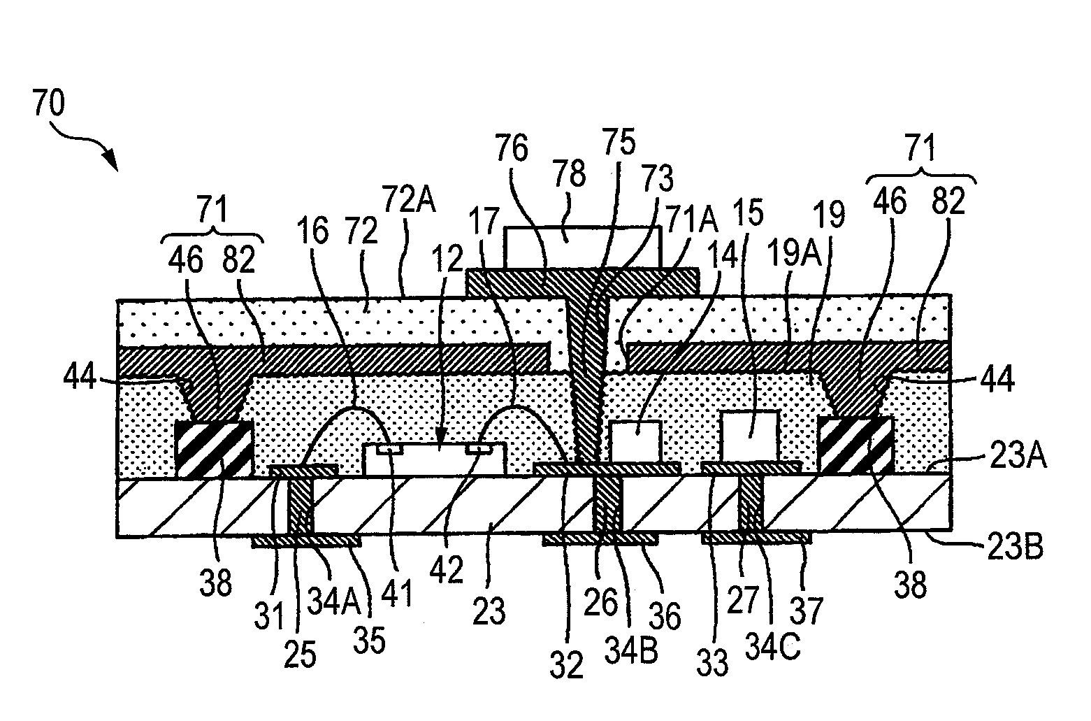
[0082]FIG. 17 is a sectional view showing a semiconductor device according to a third embodiment of the invention. In FIG. 17, the same components as those in the semiconductor device 10 according to the first embodiment have the same reference numerals.

[0083]With reference to FIG. 17, a semiconductor device 70 according to the third embodiment has the same structure as the semiconductor device 10 except that a shield layer 71 is provided in place of the shield layer 21 provided in the semiconductor device 10 according to the first embodiment, and furthermore, a buildup resin 72, an opening portion 73, a via 75, a wiring pattern 76 and an electronic component 78 are provided.

[0084]The shield layer 71 is provided on a surface of a sealing resin 19 (specifically, an upper surface 19A of the sealing resin 19 and a surface of the sealing resin 19 which constitutes an opening portion 44). The shield layer 71 has the same structure as the shield layer 21 except that a shield layer body 82...


PUM


Abstract

In a method of manufacturing a semiconductor device 10 including a wiring board 11 having a ground terminal 38, a semiconductor chip 12 and passive components 14 and 15 which are electronic components mounted on the wiring board 11, and a sealing resin 19 containing a silica filler for sealing the semiconductor chip 12 and the passive components 14 and 15, the silica filler present on a surface of the sealing resin 19 is dissolved with a hydrogen fluoride solution, and a shield layer 21 which is electrically connected to the ground terminal 38 is then formed on the surface of the sealing resin 19 by a plating method.

Description

[0001]The present invention relates to a method of manufacturing a semiconductor device, and more particularly to a method of manufacturing a semiconductor device having an electronic component mounted on a wiring board and a sealing resin containing a silica filler for sealing the electronic component.[0002]A conventional semiconductor device includes a semiconductor device (see FIG. 1) comprising an electromagnetic wave absorbing sheet having the function of blocking an electromagnetic wave.[0003]FIG. 1 is a sectional view showing the conventional semiconductor device.[0004]With reference to FIG. 1, a conventional semiconductor device 100 comprises a wiring board 101, a semiconductor chip 103 and passive components 104 and 105 which are electronic components, a sealing resin 107, and an electromagnetic wave absorbing sheet 108.[0005]The wiring board 101 has a board body 111, through vias 113 to 115 provided to penetrate through the board body 111, wiring patterns 117 to 119 provid...

Claims


Application Information

Patent Timeline
Patent Type & Authority Applications(United States)
IPC IPC(8): H01L21/56
CPCH01L23/3121H01L2924/01033H01L24/97H01L2224/48091H01L2224/48227H01L2224/97H01L2924/01011H01L2924/01029H01L2924/01078H01L2924/14H01L2924/19041H01L2924/19043H01L2924/19105H01L2924/3025H05K1/0218H05K3/284H05K3/381H05K3/4661H05K2201/0209H05K2203/0773H01L23/552H01L2924/01006H01L2924/01005H01L24/48H01L2224/85H01L2924/00014H01L2224/451H01L2924/181H01L2924/1815
Inventor FUJII, TOMOHARUSHIMIZU, YUICHIRO
Owner SHINKO ELECTRIC IND CO LTD
Why Eureka
Try Eureka