Programmed high speed deposition of amorphous, nanocrystalline, microcrystalline, or polycrystalline materials having low intrinsic defect density

a technology of microcrystalline materials and high-speed deposition, applied in chemical vapor deposition coatings, coatings, electric discharge tubes, etc., can solve the problems of many species in plasma that are ineffective and detrimental, and achieve high-speed deposition, high-quality photovoltaic materials, and limit the development of intrinsic defects

Inactive Publication Date: 2009-02-05
OVSHINSKY TECH
View PDF4 Cites 2 Cited by
  • Summary
  • Abstract
  • Description
  • Claims
  • Application Information

AI Technical Summary

Benefits of technology

[0015]This invention provides a method and apparatus for the high rate deposition of amorphous, nanocrystalline, microcrystalline, and polycrystalline semiconductors and semiconductor alloys. Materials that can be prepared according to the instant invention include the amorphous, nanocrystalline, microcrystalline, and polycrystalline forms of silicon, alloys of silicon, germanium, alloys of germanium, hydrogenated and fluorinated materials that include silicon or germanium, and combinations thereof, The target materials are particularly suitable for photovoltaic applications. The invention involves plasma deposition and focuses on controlling the growth environment of the as-deposited film to limit the development of intrinsic defects. The need for compensating agents or other reparative processing steps is thereby minimized or eliminated and high quality photovoltaic materials can be produced at deposition rates of ˜300 Å / s and higher.

Problems solved by technology

The instant method recognizes that within the distribution of species in a conventional plasma, only selected species are effective in the formation of amorphous semiconductors with low defect densities and that many species in a plasma are ineffective and detrimental because they promote the formation of defects.

Method used


Image

  • Programmed high speed deposition of amorphous, nanocrystalline, microcrystalline, or polycrystalline materials having low intrinsic defect density
  • Programmed high speed deposition of amorphous, nanocrystalline, microcrystalline, or polycrystalline materials having low intrinsic defect density
  • Programmed high speed deposition of amorphous, nanocrystalline, microcrystalline, or polycrystalline materials having low intrinsic defect density

Examples


Embodiment Construction

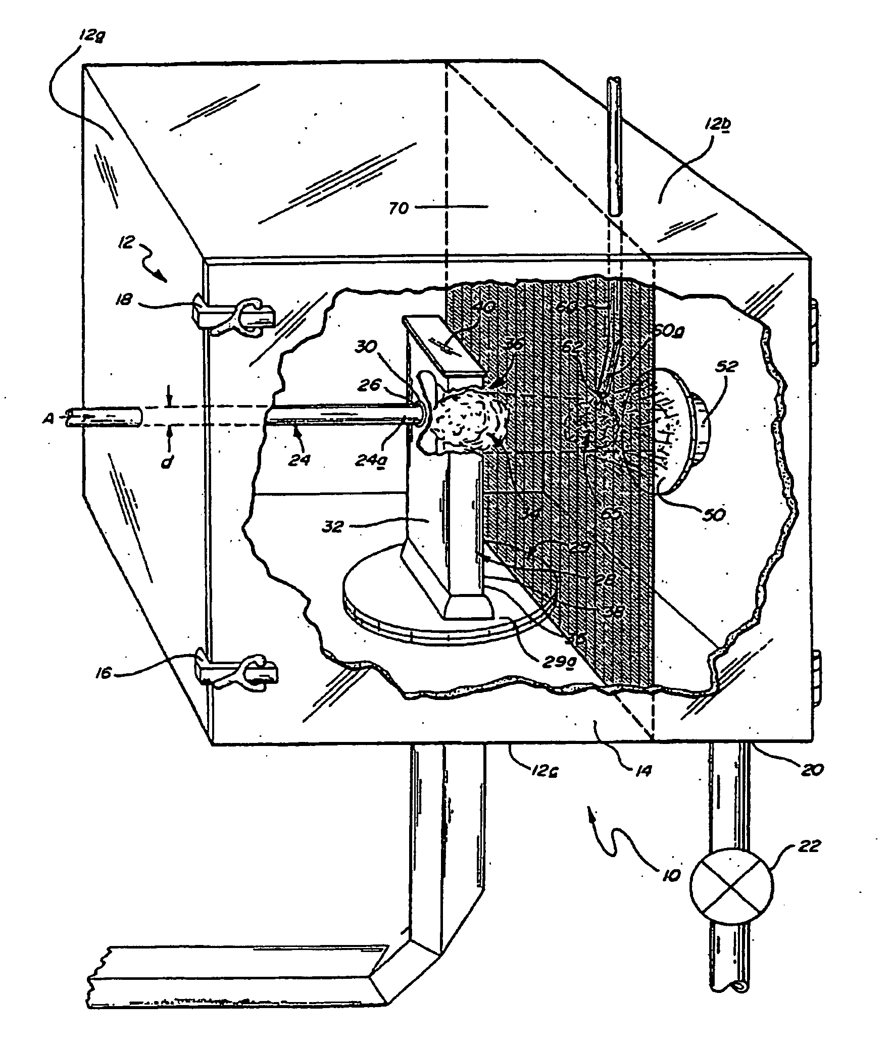
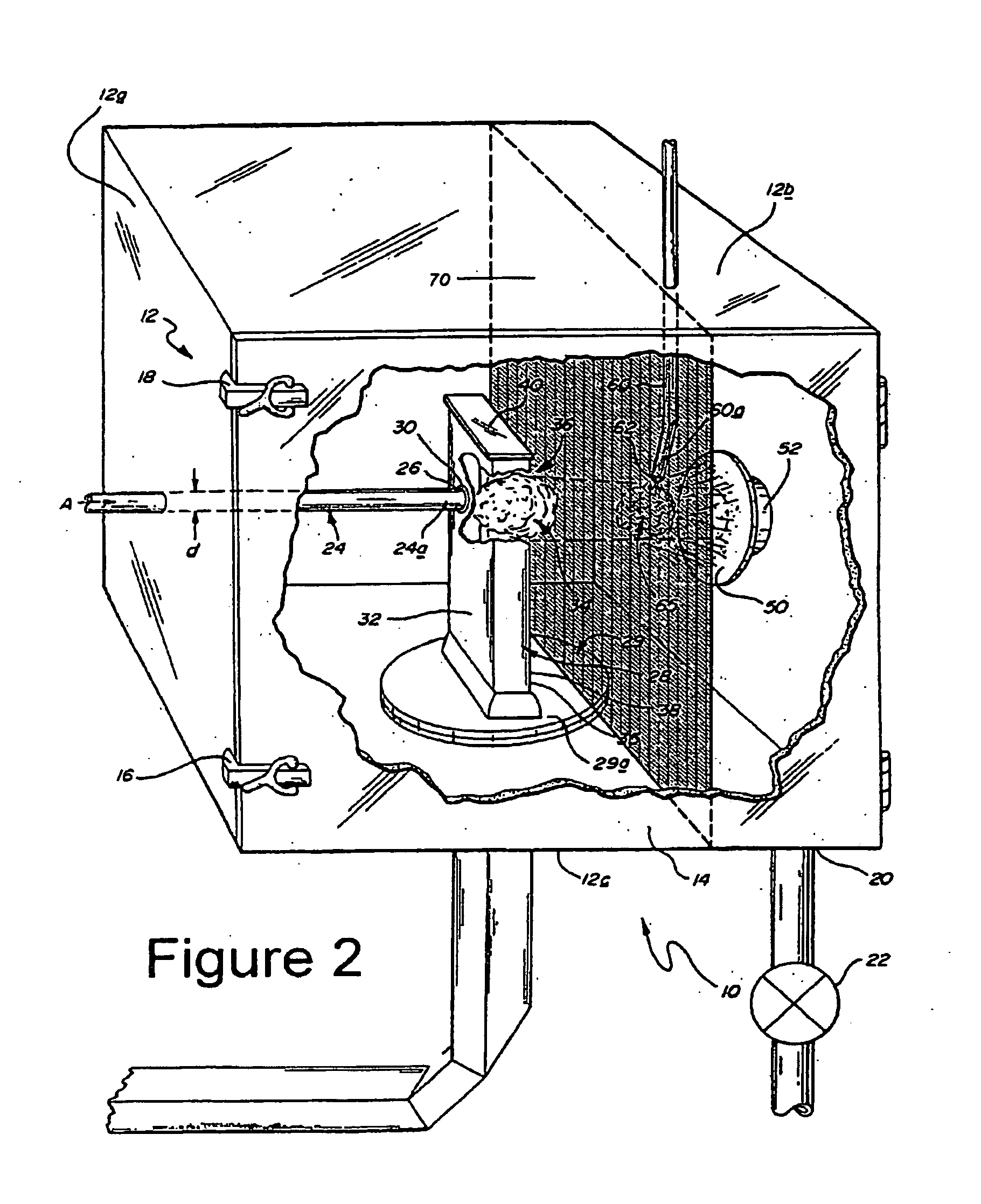
[0034]Although this invention will be described in terms of certain preferred embodiments, other embodiments that are apparent to those of ordinary skill in the art, including embodiments that do not provide all of the benefits and features set forth herein, are also within the scope of this invention. Accordingly, the scope of the invention is defined only by reference to the appended claims.

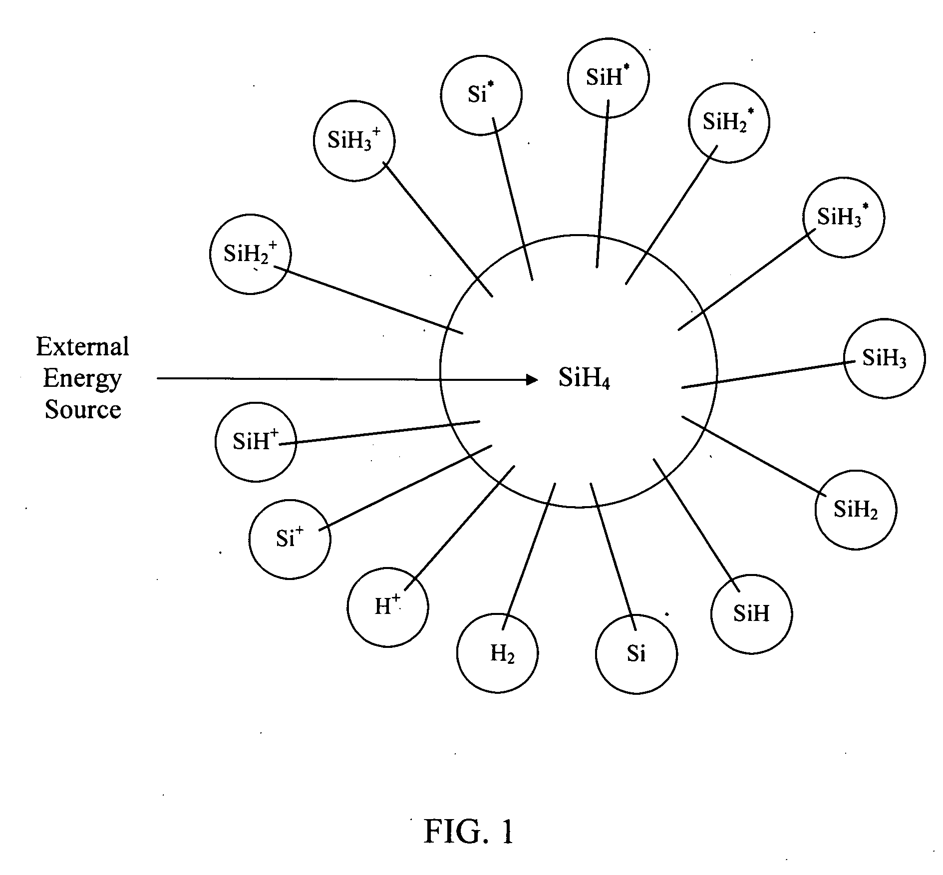
[0035]This invention provides a high deposition rate apparatus for the formation of photovoltaic materials that have a low concentration of intrinsic defects in the as-deposited state in a plasma deposition process. The invention recognizes that a conventional plasma includes many species that are detrimental to the formation of high quality photovoltaic materials. FIG. 1 depicts the distribution of the most common species in a silane (SiH4) plasma, which is used in the formation of amorphous silicon, modified forms of amorphous silicon, nanocrystalline silicon, microcrystalline silicon, and po...


PUM

PropertyMeasurementUnit
diameteraaaaaaaaaa
microwave frequencyaaaaaaaaaa
frequencyaaaaaaaaaa

Abstract

A method and apparatus for the unusually high rate deposition of thin film materials on a stationary or continuous substrate. The method includes the in situ generation of a neutral-enriched deposition medium that is conducive to the formation of thin film materials having a low intrinsic defect concentration at any speed. In one embodiment, the deposition medium is created by forming a plasma from an energy transferring gas; combining the plasma with a precursor gas to form a set of activated species that include ions, ion-radicals, and neutrals; and selectively excluding the species that promote the formation of defects to form the deposition medium. In another embodiment, the deposition medium is created by mixing an energy transferring gas and a precursor gas, forming a plasma from the mixture to form a set of activated species, and selectively excluding the species that promote the formation of defects. The apparatus has a control for the entire manufacturing process that includes a diagnostic element and a feedback control element to permit process programming to achieve and maintain the optimal distribution of one or more preferred species throughout the deposition process.

Description

RELATED APPLICATION INFORMATION[0001]This application is a continuation-in-part of U.S. patent application Ser. No. 11 / 546,619, entitled “High rate, continuous deposition of high quality amorphous, nanocrystalline, microcrystalline or polycrystalline materials” and filed on Oct. 12, 2006, the disclosure of which is incorporated by reference in its entirety herein.FIELD OF INVENTION[0002]The instant invention relates generally to an apparatus and method for the high rate deposition of high quality amorphous, nanocrystalline, microcrystalline or polycrystalline materials. More specifically, the instant invention provides an apparatus and method for scientifically tailoring the distribution of deposition intermediates to preferentially increase the concentration of intermediates conducive to the formation of photovoltaic materials that have a low concentration of intrinsic defects in the as-deposited state. Most specifically, the instant invention provides an apparatus and method for s...

Claims


Application Information

Patent Timeline
Patent Type & Authority Applications(United States)
IPC IPC(8): B05C11/00
CPCC23C16/24C23C16/27C23C16/277C23C16/452C23C16/545H01J37/32357
Inventor OVSHINSKY, STANFORD R.
Owner OVSHINSKY TECH
Why Eureka
Try Eureka