Small Area, Robust Silicon Via Structure and Process

Active Publication Date: 2009-02-05
GLOBALFOUNDRIES US INC
View PDF7 Cites 253 Cited by
  • Summary
  • Abstract
  • Description
  • Claims
  • Application Information

AI Technical Summary

Benefits of technology

[0012]Briefly, according to an embodiment of the invention a semiconductor structure includes: at least silicon substrate; one or more electronic circuits formed on each side of the at least one substrate; one or more conductive vias through the at least one substrate, each via including one or more

Problems solved by technology

It is a very complex task to develop dry etch processes that balance chemical and physical etching, since there are many parameters to adjust.
Dry etchi

Method used


Image

  • Small Area, Robust Silicon Via Structure and Process
  • Small Area, Robust Silicon Via Structure and Process
  • Small Area, Robust Silicon Via Structure and Process

Examples


Embodiment Construction

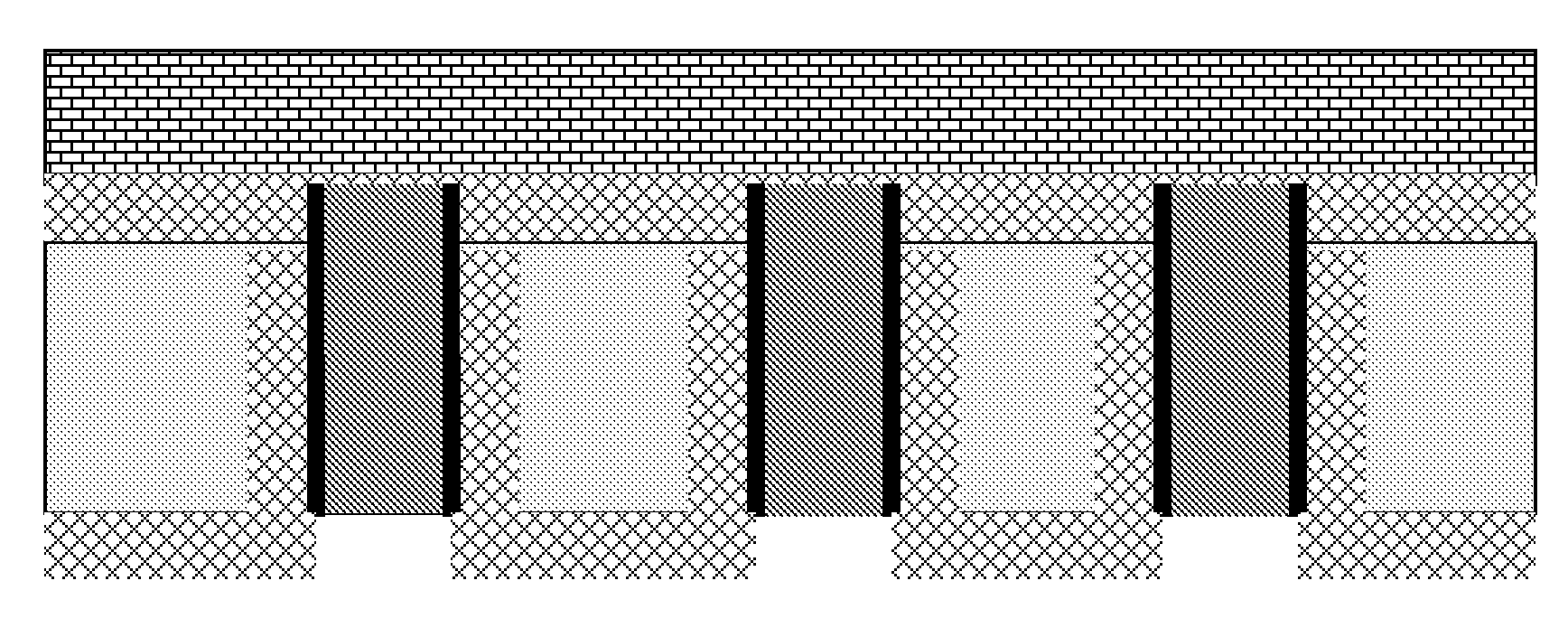
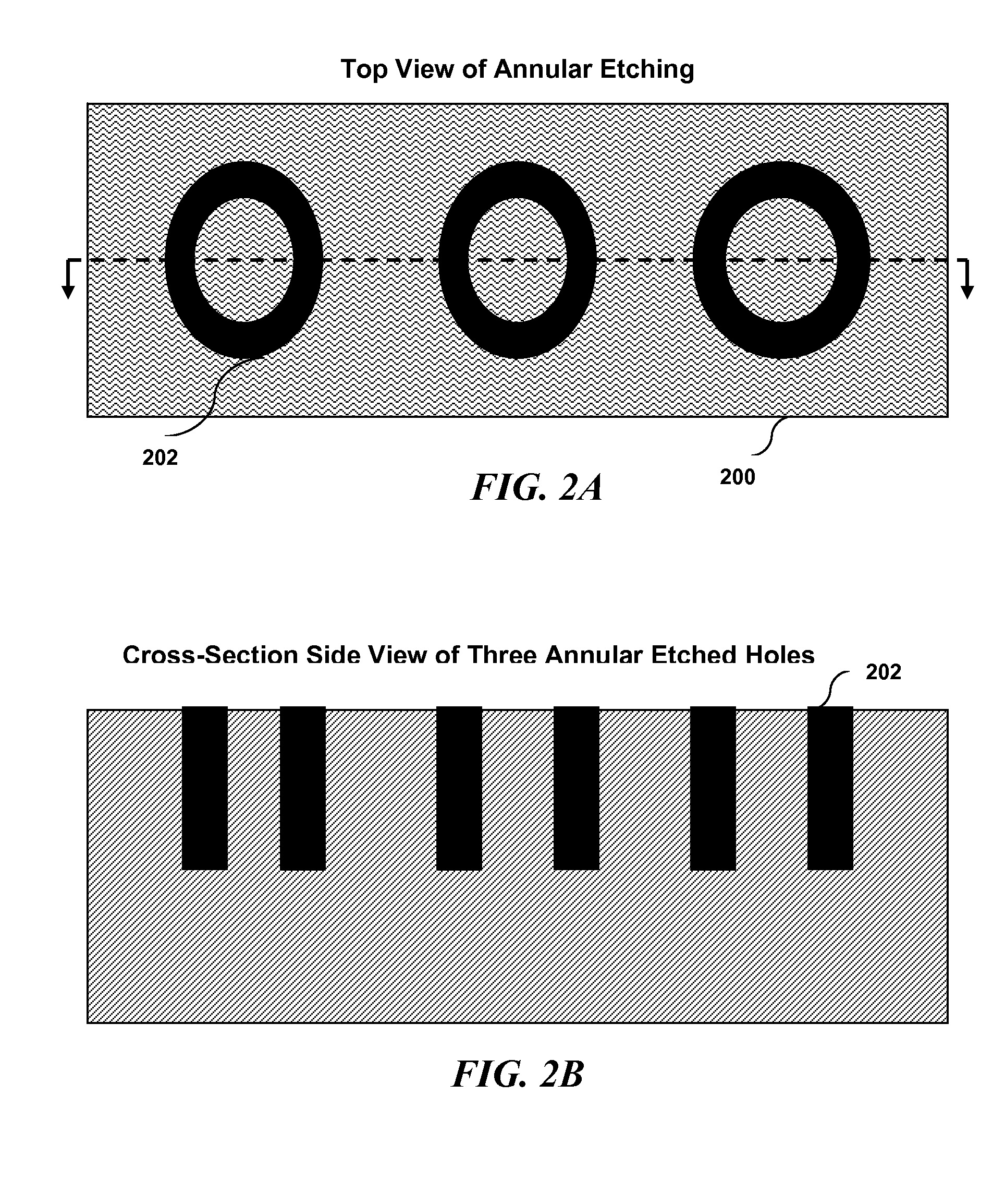
[0035]The figures and related text describe a method and structure for fabrication of silicon through vias in a small area for three-dimensional (3D) chip interconnection. The high aspect ratio via structures are capable of small area impact on circuits, and combine low stress during wafer processing with robust mechanical integrity for reliability.

[0036]According to an embodiment of the present invention, a thermal oxide dielectric with a tungsten (W) or copper (Cu) conductor is used for fabricating through vias wiring with active or passive circuits. Small vias (0.2 to 4 micron width) are prefabricated using RIE (reactive ion etching). The small size minimizes the area impact on active circuits and permits compatibility while maintaining low stress in processing 300 mm wafers. A thermal oxide collar is then applied to the vias. After the formation of the thermal oxide collar, the active circuits, trench capacitors and wiring integration can be fabricated.

[0037]Prefabrication of th...


PUM


Abstract

A semiconductor structure includes: at least one silicon surface wherein the surface can be a substrate, wafer or other device. The structure further includes at least one electronic circuit formed on each side of the at least one surface; and at least one conductive high aspect ratio through silicon via running through the at least one surface. Each through silicon via is fabricated from at least one etch step and includes: at least one thermal oxide dielectric for coating at least some of a sidewall of the through silicon via for a later etch stop in fabrication of the through silicon via.

Description

STATEMENT REGARDING FEDERALLY SPONSORED-RESEARCH OR DEVELOPMENT[0001]The invention described herein was funded in part by a grant from the National Security Agency DARPA Program, Contract No. H98230-04-C-0920, and in part by DARPA, Contract No. NBCH3039004. The United States Government may have certain rights under the invention.CROSS-REFERENCE TO RELATED APPLICATIONS[0002]Not applicable.INCORPORATION BY REFERENCE OF MATERIAL SUBMITTED ON A COMPACT DISC[0003]Not Applicable.FIELD OF THE INVENTION[0004]The present invention broadly relates to the field of silicon wafer etching and more particularly relates to the field of deep etching of silicon using a reactive process.BACKGROUND OF THE INVENTION[0005]In silicon chip etching, a hole, or via, is machined through a substrate (die) or through multiple stacked dice to create a path for the interconnects. For some silicon chips, many holes must be etched on a very small surface. Additionally, the holes must have a high aspect ratio (deep,...

Claims


Application Information

Patent Timeline
IPC IPC(8): H01L21/768H01L23/52
CPCH01L21/76898H01L24/03H01L2924/0002H01L2924/1461H01L2224/0401H01L2224/0557H01L2924/10253H01L2924/014H01L2924/01074H01L24/05H01L24/11H01L24/13H01L24/80H01L24/94H01L2224/13025H01L2224/16H01L2224/94H01L2924/01029H01L2924/01073H01L2924/01078H01L2924/01079H01L2924/01082H01L2924/19041H01L2924/19042H01L2924/30105H01L2924/30107H01L2924/01006H01L2924/01033H01L2924/01072H01L2224/11H01L2924/00H01L2224/05552
Inventor ANDRY, PAUL S.COTTE, JOHN M.KNICKERBOCKER, JOHN ULRICHTSANG, CORNELIA K.
Owner GLOBALFOUNDRIES US INC
Why Eureka
Try Eureka