
Chemical mechanical polishing apparatus and chemical mechanical polishing method thereof

Inactive Publication Date: 2009-02-05
NAT TAIWAN UNIV OF SCI & TECH
View PDF20 Cites 2 Cited by
  • Summary
  • Abstract
  • Description
  • Claims
  • Application Information

AI Technical Summary

Benefits of technology

[0013]The invention is directed to a chemical mechanical polishing apparatus and a chemical mechanical polishing method thereof. By way of adjusting the positive pressure, the chemical mechanical polishing apparatus and the chemical mechanical polishing method thereof at least have the advantages of avoiding dishing effect and erosion effect and preventing the low-K material and the copper material from being detached.

Problems solved by technology

When the difference between the protrusion and the indention on the surface of the wafer is too large, the focusing precision during the optical-lithography manufacturing process will be severely affected.
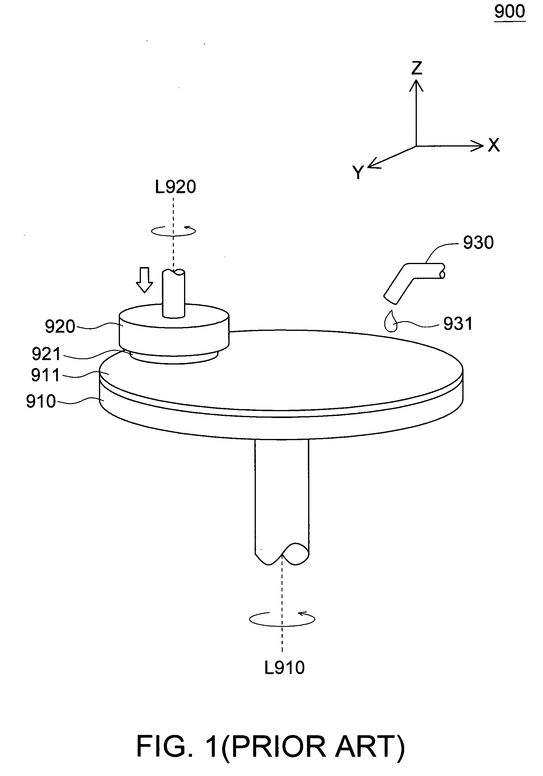
However, as the wire density keeps increasing but the wire pitch keeps decreasing, conventional chemical mechanical polishing apparatus 900 and polishing method thereof encounter many problems that are hard to be resolved.
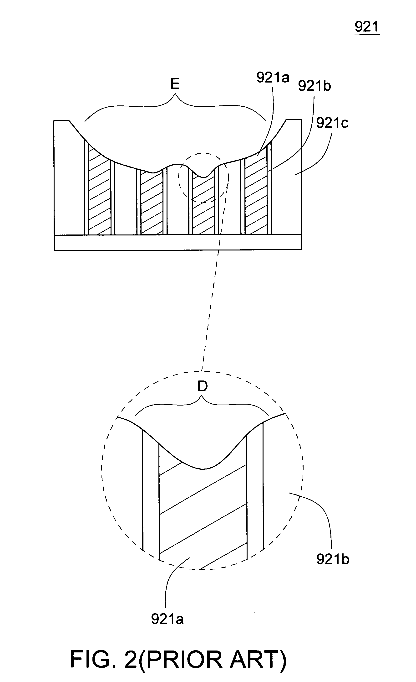
Firstly, there comes dishing effect problem.
The RC-delay effect reduces signal transmission rate and increases cross talk noise and power consumption.
The copper wire 921a has a lower hardness level and is not easy to form a protective oxidation layer.
Secondly, there comes the erosion effect problem.
During the polishing manufacturing process, the insulating layer 921c are often over polished and resulted in erosion effect E.
Thirdly, the throughout is decreases.
During the polishing manufacturing process, the dishing effect D and the erosion effect E often occur concurrently, largely affecting the defect rate of the product.
Fourthly, manufacturing process is difficult to be integrated.
However, the low-K material has low stiffness, low fracture to ugliness, low hardness and instability.
Therefore, during the polishing manufacturing process, the low-K material is likely to be adhered onto hetero material and results in detachment.
Fifthly, the yield rate decreases and cost increases.
Conventional chemical mechanical polishing apparatus 900 and the polishing method thereof often result in defected products which cannot be repaired and are wasted, not only reducing the yield rate but also increasing manufacturing cost.

Method used


Image

  • Chemical mechanical polishing apparatus and chemical mechanical polishing method thereof
  • Chemical mechanical polishing apparatus and chemical mechanical polishing method thereof
  • Chemical mechanical polishing apparatus and chemical mechanical polishing method thereof

Examples


first embodiment

[0035]Referring to FIG. 3, a perspective of a chemical mechanical polishing apparatus 100 according to a first embodiment of the invention is shown. The chemical mechanical polishing apparatus 100 includes a carrier 110, a polishing platen 120, a polishing slurry injector 130 and a controlling unit 140. The carrier 110 used for carrying a wafer 111 drives the wafer 111 to revolve around a first central axis L110. The polishing platen 120 is used for pasting a polishing pad 121 thereon. In the present embodiment of the invention, the polishing platen 120 is located underneath the carrier 110 and is larger than the carrier 110. A positive pressure F is applied between the carrier 110 and the polishing platen 120 for enabling the polishing pad 121 and the wafer 111 to contact each other tightly. The polishing platen 120 drives the polishing pad 121 to revolve around a second central axis L120. Generally speaking, the polishing pad 121 and the carrier 110 are rotated in opposite directi...

second embodiment

[0052]Referring to FIG. 7, a perspective of a chemical mechanical polishing apparatus 200 according to a second embodiment of the invention is shown. The chemical mechanical polishing apparatus 200 of the present embodiment of the invention differs with the chemical mechanical polishing apparatus 100 of the first embodiment in that the chemical mechanical polishing apparatus 200 further includes a flatness sensor 250 and at least a supplementary polishing platen 260. The supplementary polishing platen 260 is used for pasting a supplementary polishing pad 261 thereon. In the present embodiment of the invention, the carrier 210 and the wafer 211 are disposed at the bottom while the polishing platen 220, the polishing pad 221, the supplementary polishing platen 260 and the supplementary polishing pad 261 are disposed at the top. As for other similarities, the same designations are used and are not repeated here.

[0053]Referring to both FIG. 7 and FIG. 8. FIG. 8 is a flowchart of a chemi...

third embodiment

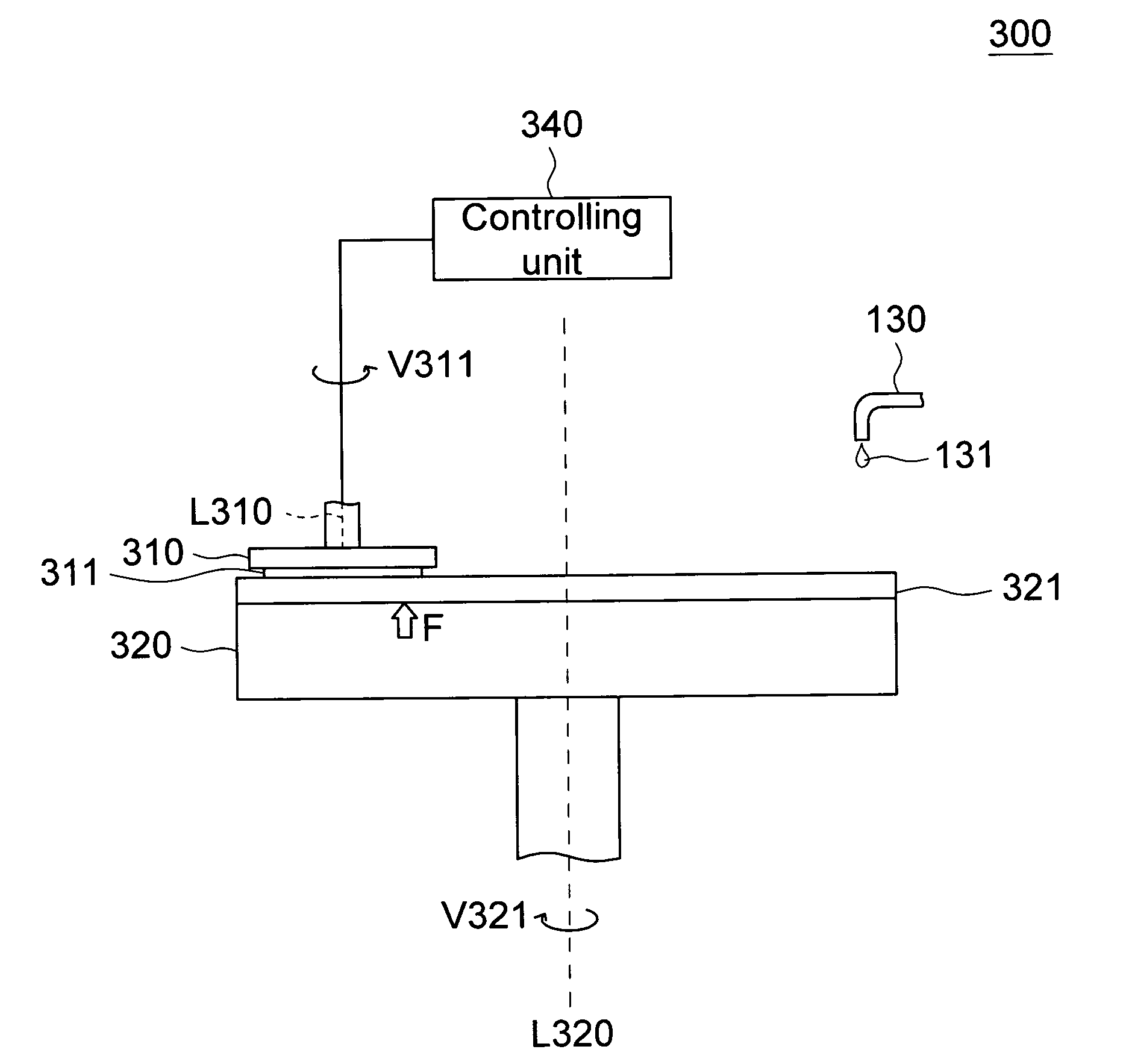
[0054]Referring to FIG. 9, a perspective of the chemical mechanical polishing apparatus 300 according to a third embodiment of the invention is shown. The carrier 310 drives the wafer 311 to revolve at a first rotation rate V311, and the poishing platen 320 drives the polishing pad 321 to revolve at a second rotation rate V321.

[0055]Referring to FIG. 10A and FIG. 10B. FIG. 10A is a top view of the wafer 311. FIG. 10B is a side view of the wafer 311. As indicated in FIG. 10A, the wafer 311 has N wafer sub-regions Wi′i=1˜N. As indicated in FIG. 10B, each wafer sub-region Wi has a first thickness d1i′i=1˜N. As the surface of the wafer 311 is not even, the first thickness d1i′i=1˜N is not identical.

[0056]Referring to FIGS. 11A-11B, various side views of the wafer 311 and the polishing pad 321 are shown. During the rotation of the wafer 311 and the polishing pad 321, the position at which a wafer sub-region Wi′i=1˜N contacts the polishing pad 321 keeps changing. At a particular time t, t...


PUM

PropertyMeasurementUnit
Thicknessaaaaaaaaaa
Dielectric polarization enthalpyaaaaaaaaaa
Pressureaaaaaaaaaa

Abstract

A chemical mechanical polishing apparatus and a chemical mechanical polishing method thereof are provided. The chemical mechanical polishing method at least includes the following steps. In step a, a positive pressure is formed between a polishing pad and a wafer. In step b, the wafer is driven to revolve around a first central axis. In step c, a polishing slurry is injected between the polishing pad and the wafer. In step d, the positive pressure formed on the wafer by the polishing pad is adjusted for change the contacting modes of the polishing pad and the wafer as well as the wafer removal rate.

Description

[0001]This application claims the benefit of Taiwan application Serial No. 96128302, filed Aug. 1, 2007, and Taiwan application Serial No. 97108401, filed Mar. 10, 2008, the subject matter of which is incorporated herein by reference.BACKGROUND OF THE INVENTION[0002]1. Field of the Invention[0003]The invention relates in general to a chemical mechanical polishing apparatus and a chemical mechanical polishing method thereof, and more particularly to a chemical mechanical polishing apparatus for polishing the wafer and a chemical mechanical polishing method thereof.[0004]2. Description of the Related Art[0005]For semiconductor elements, the wire density is increasing but the wire pitch is decreasing, the flatness on the surface of the wafer must be maintained at a certain level. When the difference between the protrusion and the indention on the surface of the wafer is too large, the focusing precision during the optical-lithography manufacturing process will be severely affected. Dur...

Claims


Application Information

Patent Timeline
IPC IPC(8): B24B49/04B24B29/02B24B49/08
CPCB24B37/042B24B49/16B24B37/107
Inventor CHEN, CHAO-CHANGHSU, LI-SHENG
Owner NAT TAIWAN UNIV OF SCI & TECH
Learn More