Logic Circuit and Single-Electron Spin Transistor

a logic circuit and transistor technology, applied in the field of logic circuits and single-electron spin transistors, can solve the problems of large current consumption and the area of each transistor, large area of logic circuits, and large number of elements, so as to reduce the carrier density, the effect of reducing the power consumption of changing the magnetization direction of the island and facilitating the change of the magnetization direction

Inactive Publication Date: 2009-02-12
JAPAN SCI & TECH CORP
View PDF5 Cites 14 Cited by
  • Summary
  • Abstract
  • Description
  • Claims
  • Application Information

AI Technical Summary

Benefits of technology

[0010]It is therefore an object of the present invention to provide a logic circuit that can reconfigure the functions of a logic circuit in a nonvolatile manner and has a small circuit area and small power consumption, and to provide single-electron spin transistors.
[0011]The present invention provides a logic circuit that includes a single-electron spin transistor that has a source, a drain, an island that is provided between the source and the drain, and a gate that is capacitively coupled to the island, a tunnel junction being provided between the source and the island, another tunnel junction being provided between the drain and the island. In this logic circuit, at least one of the source, the drain, and the island includes a ferromagnetic material having a reversible magnetization direction. In accordance with the present invention, the conductance between the source and the drain can be controlled by changing the magnetization direction of the single-electron spin transistor. By doing so, a logic circuit that can reconfigure functions in a nonvolatile manner can be provided. Further, as the single-electron spin transistor is employed, a logic circuit that has a small circuit area and small power consumption can be provided.

Problems solved by technology

However, those circuits have the problems of being volatile and having a large number of elements.
A spin MOSFET, however, is based on a MOSFET and involves a large charge amount.
As a result, the area of the logic circuit becomes large.
Moreover, since a spin MOSFET is based on a MOSFET, the current consumption and the area of each transistor are large.

Method used


Image

  • Logic Circuit and Single-Electron Spin Transistor
  • Logic Circuit and Single-Electron Spin Transistor
  • Logic Circuit and Single-Electron Spin Transistor

Examples


first embodiment

[0102]A first embodiment is an example of an inverter circuit that can control the logic threshold value in a nonvolatile manner, by varying the variable magnetization direction of each SEST.

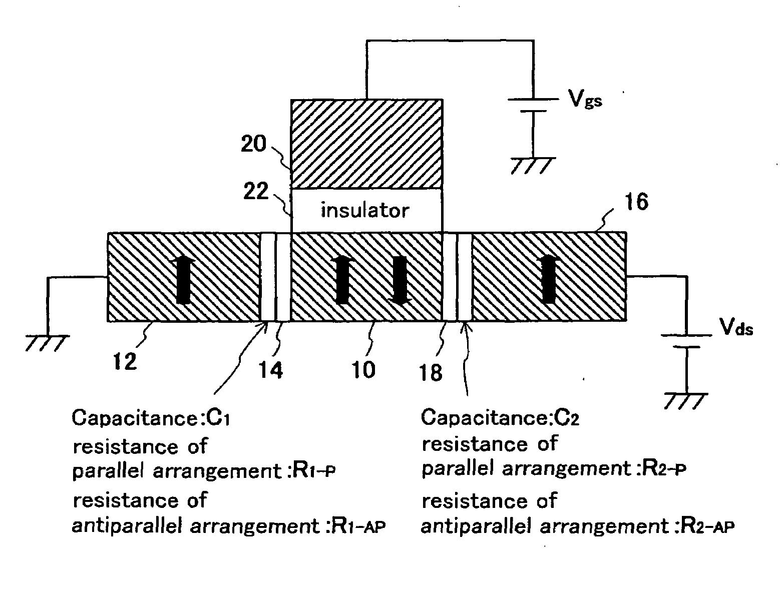
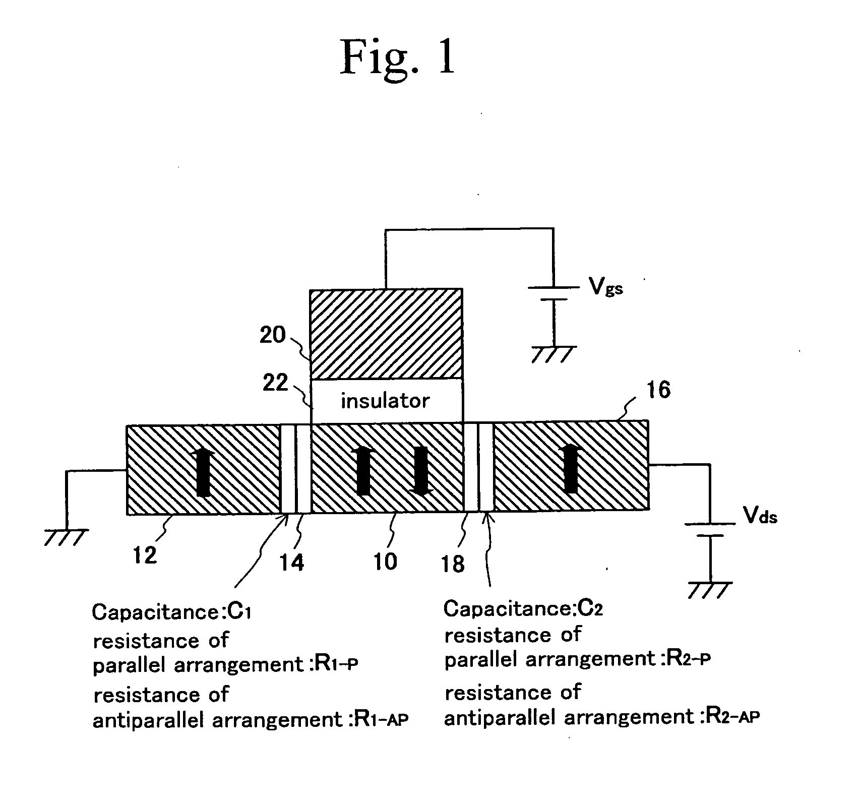
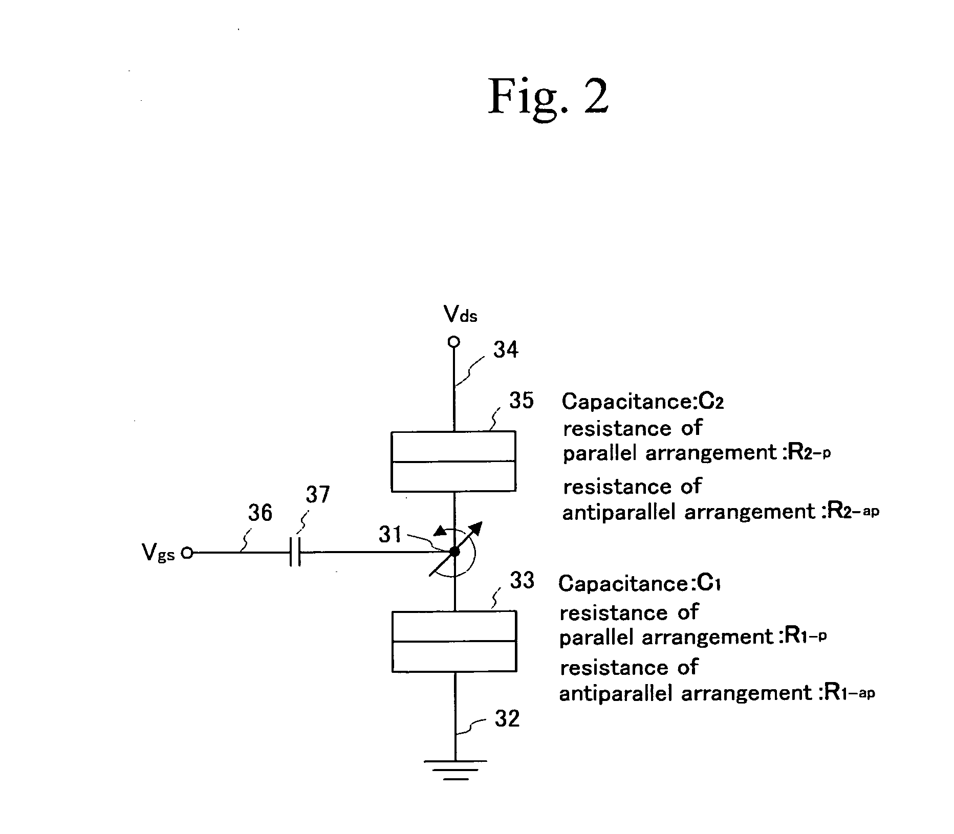
[0103]FIG. 10 shows a circuit diagram of the inverter circuit in accordance with the first embodiment. This inverter circuit (the first inverter circuit) includes a SEST1 (100) and a SEST2 (110). The source 102 of the SEST1 (100) is connected to an output terminal 122, and the drain 104 is connected to a first power supply terminal 128. Tunnel junctions 103 and 105 are provided between an island 101 and the source 102 and between the island 101 and the drain 104, respectively. The tunnel junctions 103 and 105 have capacitance values C2 and C1, resistance values R2-p and R1-p in the parallel arrangement, and resistance values R2-ap and R1-ap in the antiparallel arrangement. A gate 106 is connected to an input terminal 120. A control gate 108 is grounded. The capacitance value of a gate capacitanc...

second embodiment

[0112]A second embodiment is an example of a logic circuit that can reconfigure an OR / AND circuit function using SESTs in a nonvolatile manner. FIG. 13 is a circuit diagram of the logic circuit in accordance with the second embodiment. This logic circuit includes a first inverter circuit (INV1) 190 and a second inverter circuit (INV2) 194. The first inverter circuit (INV1) 190 includes a SEST1 (130) and a SEST2 (140). The INV1 (190) has the same circuit structure and functions as the inverter circuit of the first embodiment, except that a first input terminal and a second input terminal are provided, and an analog input is to be input.

[0113]The structure of the logic circuit is now described in greater detail. The source 132 of the SEST1 (130) is connected to an output terminal 152 of the INV1 (190), and the drain 134 is connected to a first power supply terminal 158. Tunnel junctions 133 and 135 are provided between an island 131 and the source 132 and between the island 131 and th...

third embodiment

[0129]A third embodiment is an example of an asymmetrical logic circuit including SESTs. First, the principles of this embodiment are described. The broken line in FIG. 17 indicates the input / output curve of the inverter circuit of the first embodiment shown in FIG. 11 in a case where the magnetization arrangement of each of the SEST1 (100) and the SEST2 (110) is the parallel arrangement (P). In such a case, the inverter circuit becomes an inverter having a logic threshold value of 0.5.

[0130]In a case where an input is equal to or smaller than “0.5” (V1), the output is greater than “0.5”. When an inverter circuit having an A-D converter function is connected in the next stage, almost “0” can be output. In a case where the input is equal to or greater than “0.5” (V2), the output is smaller than “0.5”. When an inverter circuit having an A-D converter function is connected in the next stage, almost “1” can be output.

[0131]In a case where the magnetization arrangement of the SEST1 (100)...


PUM


Abstract

A logic circuit that can reconfigure its functions in a nonvolatile manner and a single-electron transistor to be used in the logic circuits are provided. The logic circuit has a single-electron spin transistor that includes: a source; a drain; an island that is provided between the source and the drain, and has tunnel junctions between the island and the source and drain; and a gate that is capacitively coupled to the island. In this logic circuit, at least one of the source, the drain, and the island includes a ferromagnetic material having a variable magnetization direction.

Description

FIELD OF THE INVENTION[0001]The present invention relates to logic circuits and single-electron spin transistors, and more particularly, to a logic circuit that can reconfigure its functions and single-electron spin transistorsBACKGROUND OF THE INVENTION[0002]Having short development cycles, logic circuits that can reconfigure functions according to programs have been used for mobile devices such as portable telephone devices having short product development cycles. Also, such logic circuits have been studied as the key devices of information systems with reprogrammable hardware. Reconfigurable logic circuits include circuits having FPGAs (Field Programmable Logic Arrays) of the LUT (Look Up Table) type or νMOS circuits. However, those circuits have the problems of being volatile and having a large number of elements.[0003]To solve those problems, a circuit including spin transistors having spin-dependent conductivity, such as spin MOSFETs, is disclosed in Non-Patent Reference 1. Th...

Claims


Application Information

Patent Timeline
Patent Type & Authority Applications(United States)
IPC IPC(8): H01L29/76
CPCB82Y10/00H03K19/08H01L29/7613H01L29/66984
Inventor TANAKA, MASAAKISUGAHARA, SATOSHIPHAM, HAI NAM
Owner JAPAN SCI & TECH CORP
Why Eureka
Try Eureka