Method for producing nanowires using porous glass template, and multi-probe, field emission tip and devices employing the nanowires

a nanowire and template technology, applied in the manufacture of electrode systems, electric discharge tubes/lamps, discharge tubes luminescent screens, etc., can solve the problems of inability to apply mass production, complicated conventional methods for producing nanowires using templates, and inability to meet the requirements of mass production, etc., to achieve the effect of easy control

Inactive Publication Date: 2009-02-19
SAMSUNG ELECTRONICS CO LTD
View PDF13 Cites 45 Cited by
  • Summary
  • Abstract
  • Description
  • Claims
  • Application Information

AI Technical Summary

Benefits of technology

[0024]In accordance with still another exemplary embodiment of the present invention, provided is a device comprising a field emission tip, which can be readily controlled on a nanoscale with regard to size, length and density.

Problems solved by technology

Whereas extensive and active research is now being made into the physical properties and methods of producing nanoparticles, nanowires have received little study.
However, these conventional methods for producing nanowires using a template can be complicated and require too much time to be applied for mass production.
In addition, they can suffer from the disadvantage of being unable to produce highly straight and precisely arranged nanowires.
Also, the template cannot be applied for the production of optical elements because it is not transparent.
The nanowires obtained through this process, however, can have low linear densities and a large diameter of 40 nm or greater, and can be non-uniform in length and diameter.

Method used


Image

  • Method for producing nanowires using porous glass template, and multi-probe, field emission tip and devices employing the nanowires
  • Method for producing nanowires using porous glass template, and multi-probe, field emission tip and devices employing the nanowires
  • Method for producing nanowires using porous glass template, and multi-probe, field emission tip and devices employing the nanowires

Examples


example 1

Production of Nanowires (1)

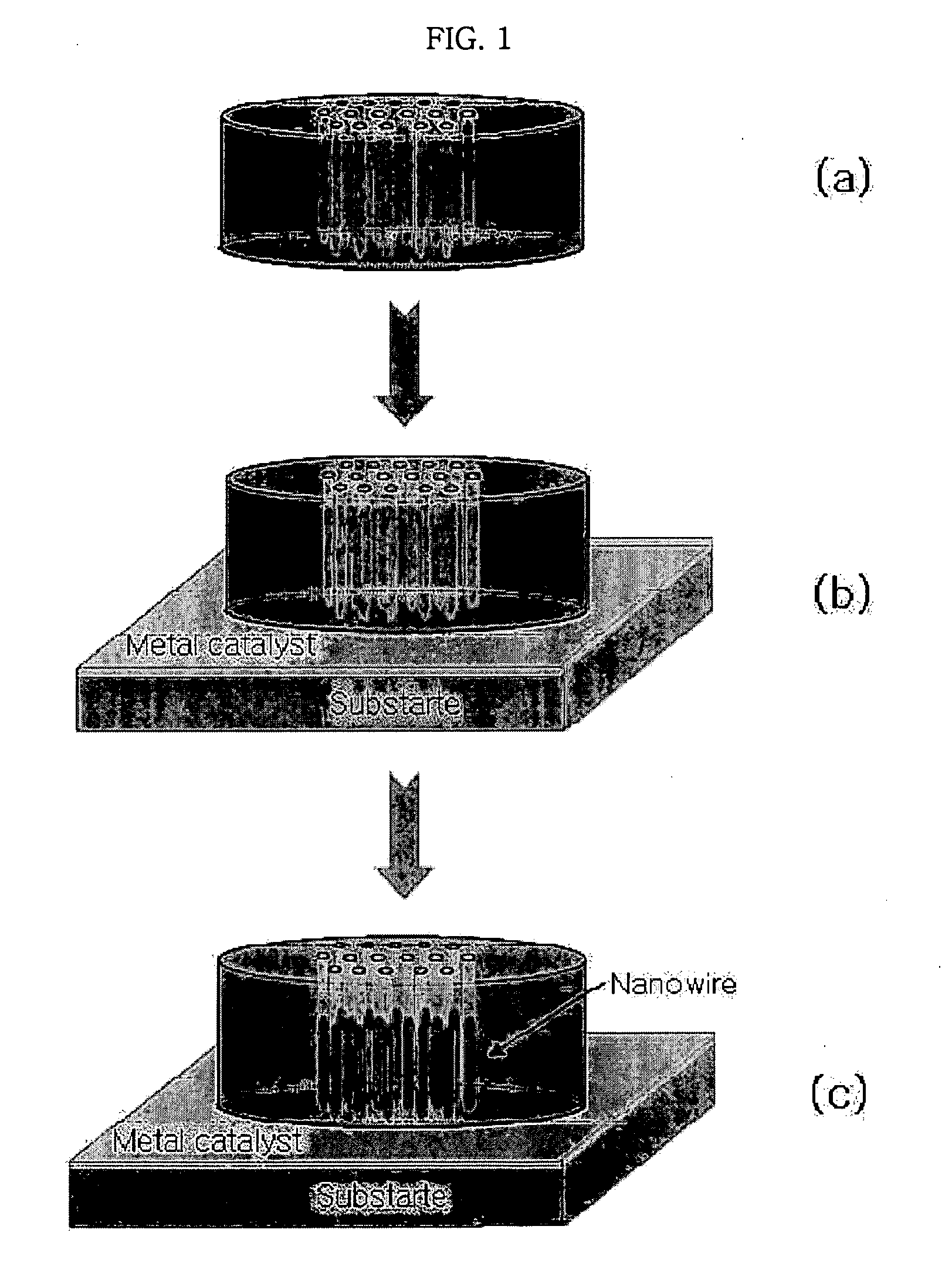
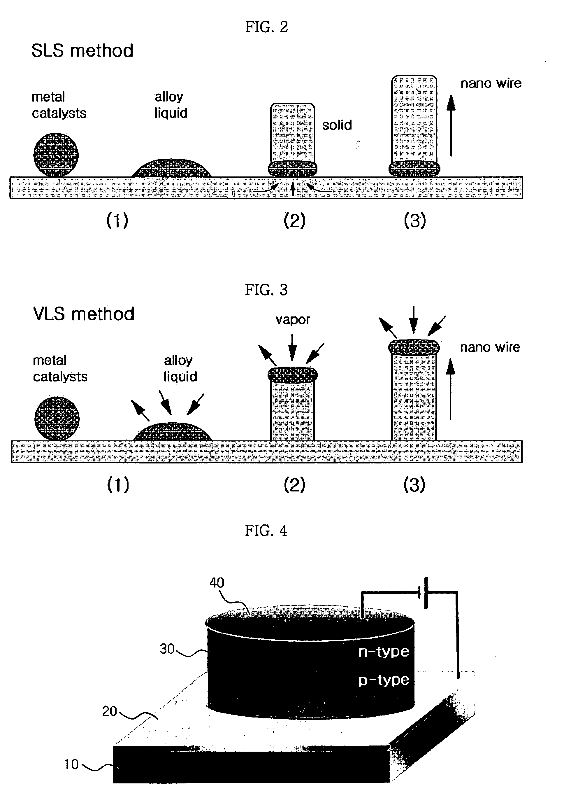
[0092]Following the removal of spontaneous oxides from a p-doped silicon substrate using an organic detergent and hydrofluoric acid, Au nanoparticles, serving as catalysts, commercially available from Nipponpaint, were spin-coated to form a thin film about 10 nm thick. Subsequently, a glass template was placed on the substrate, which was then introduced into a furnace. The temperature of the furnace was increased at a rate of 10 to 15° C. per minute, and Ar was introduced at a speed of 100 sccm through a sieve, with the total process pressure maintained at 500 torr. When heated to the process temperature 1,000° C., the substrate was maintained thereat for 30 minutes so as to grow the nanowires, followed by slowly cooling the substrate to 700° C. to terminate the growth of the nanowires.

example 2

Production of Nanowires (2)

[0093]The same procedure as in Example 1 was conducted, with the exception that a 4% SiH4 gas was further introduced at a speed of 100 sccm in addition to Ar gas, and the process temperature was set at 400° C.

example 3

Fabrication of Multi-Probe

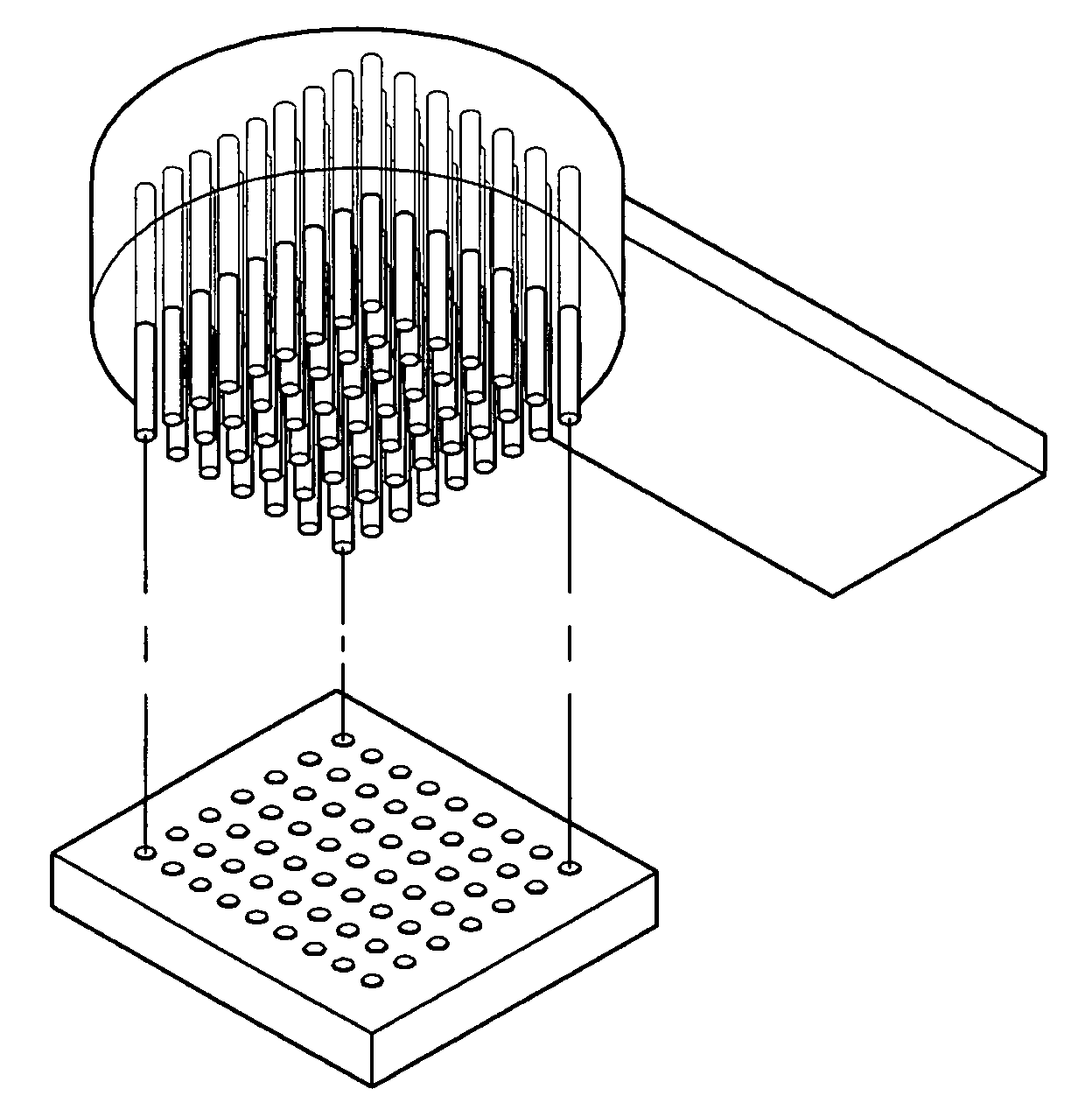
[0094]The template of the nanowires produced in Example 1 was coated with a photoresist composition containing AZ1512, and a partial terminal region of the template was then exposed using a g-line stepper. The exposed region of the template was etched using a hydrofluoric acid solution to partially expose the microwires confined within the pores.


PUM

PropertyMeasurementUnit
thicknessaaaaaaaaaa
temperatureaaaaaaaaaa
pressureaaaaaaaaaa

Abstract

Disclosed herein is a method for producing nanowires, which features the use of a porous glass template in combination with a solid-liquid-solid or vapor-liquid-solid process for growing nanowires which are highly straight and have nanoparticles precisely arranged therein. The nanowires can be grown into composite structures of superlattices and hybrids by modulating the composition of the materials provided thereto. Also disclosed is the use of the nanowires in multi-probes, field emission tips, and devices.

Description

CROSS-REFERENCE TO RELATED PATENT APPLICATIONS[0001]This application claims priority to Korean Patent Application No. 10-2005-0107443, filed on Nov. 11, 2005; Korean Patent Application No. 10-200640034947, filed on Apr. 18, 2006; and Korean Patent Application No. 10-2006-0036130, filed on Apr. 21, 2006 in the Korean Intellectual Property Office, the disclosures of which are incorporated herein in their entireties by reference.BACKGROUND OF THE INVENTION[0002]1. Field of the Invention[0003]The present invention relates to a method for producing nanowires using a porous glass template, and the nanowires. More particularly, the present invention relates to a method for producing nanowires using a porous glass template in combination with a solid-liquid-solid (SLS) or a vapor-liquid-solid (VLS) technique, and nanowires which are grown in highly straight directions and have nanoparticles well arranged therein. Also, the present invention is concerned with a multi-probe, a field emission ...

Claims


Application Information

Patent Timeline
Patent Type & Authority Applications(United States)
IPC IPC(8): H01J1/62H01J1/02H01L21/28
CPCB82Y10/00H01L29/22H01J9/025H01J2329/0431H01J2329/0455H01L21/02381H01L21/02521H01L21/02573H01L21/02603H01L21/02606H01L21/02642H01L21/02645H01L21/02653H01L29/0665H01L29/0673H01L29/0676H01L29/16H01L29/1608B82Y30/00
Inventor LEE, EUN KYUNGCHOI, BYOUNG LYONGKIM, JONG MINKWON, SOON JAECHO, KYUNG SANGLEE, JAE HO
Owner SAMSUNG ELECTRONICS CO LTD
Why Eureka
Try Eureka