Magnetic sensor and manufacturing method of the same

a technology of magnetic sensor and manufacturing method, which is applied in the field of magnetic sensor, can solve the problems of difficult to reduce the size of the magnetic sensor, the inability of the magnetic sensor itself to be reduced in size, and the inability to reduce the area, so as to reduce the size and cost, suppress the increase in the height of the sensor, and reduce the mount area

Active Publication Date: 2009-02-19
SAE MAGNETICS (HK) LTD +1
View PDF2 Cites 21 Cited by
  • Summary
  • Abstract
  • Description
  • Claims
  • Application Information

AI Technical Summary

Benefits of technology

[0024]As in the above, it is possible to provide the magnetic sensor that can be reduced in size and cost by manufacturing the magnetic sensor through the above-described manufacturing method.
[0025]The present invention is structured and functions in the manner described above. With the present invention, it is possible to manufacture the magnetic sensor by having the output terminal of the magnetic field detection chip arranged not to face in the height direction of the magnetic sensor when the magnetic field detection chip is mounted on the substrate. Thus, when the output terminal of the magnetic field detection chip and the connection terminal of the substrate are connected, the connected part in the output terminal is not formed in the height direction of the magnetic sensor. Therefore, it is possible to suppress an increase in the height of the sensor. Further, since the distance between the terminals connected between the magnetic field detection chip and the substrate can be made closer, it is possible to reduce the mount area and to simplify the connection thereof. As described above, the present invention can achieve such excellent effects that the size of the magnetic sensor itself can be reduced and the cost of the products can be reduced by simplifying the manufacture process and improving the efficiency thereof, which have not bee achieved conventionally.

Problems solved by technology

Thus, it is necessary to provide a space for a wire 513, which may result in having such a problem that the magnetic sensor itself cannot be reduced in size.
That is, height h and the area cannot be reduced when the GMR chip 501 is mounted, so that it is difficult to reduce the size of the magnetic sensor.
However, the magnetic sensor is also formed higher for the height of the gold ball 503 (code h′), so that there still remains the issue that the magnetic sensor cannot be reduced in size.

Method used


Image

  • Magnetic sensor and manufacturing method of the same
  • Magnetic sensor and manufacturing method of the same
  • Magnetic sensor and manufacturing method of the same

Examples


first embodiment

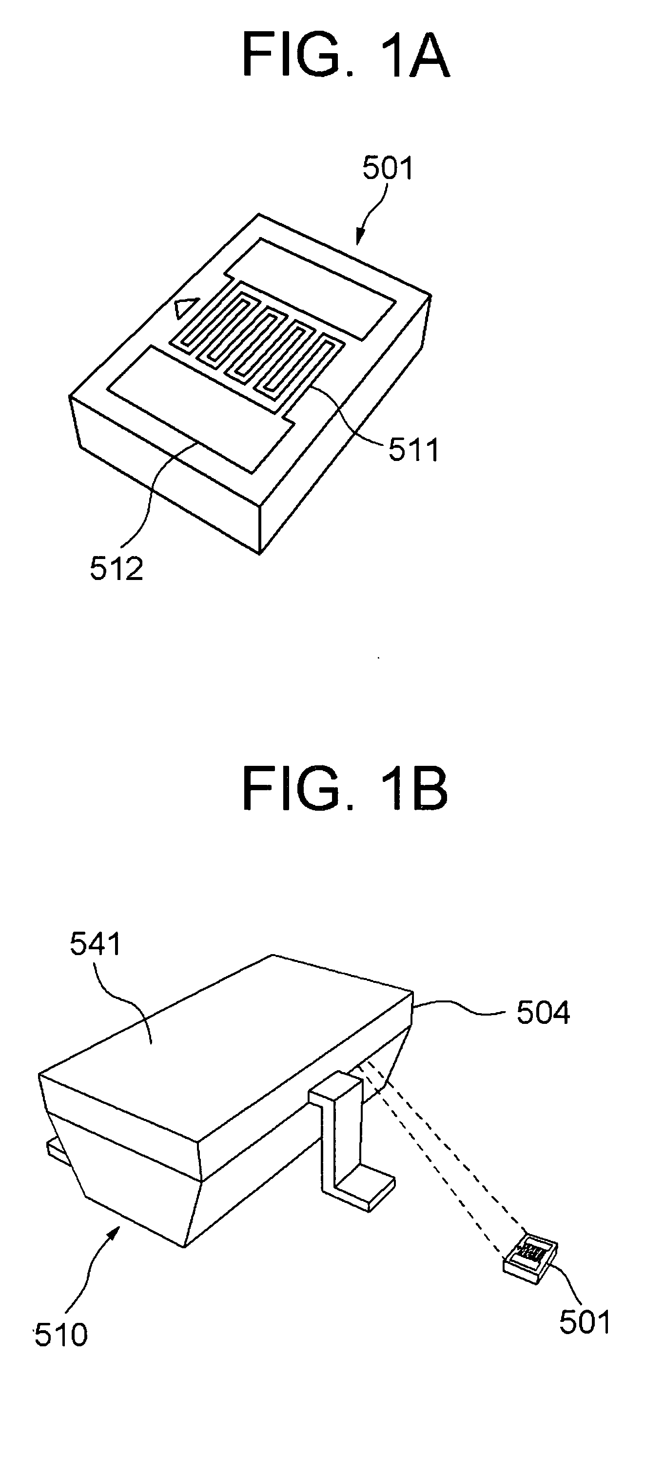
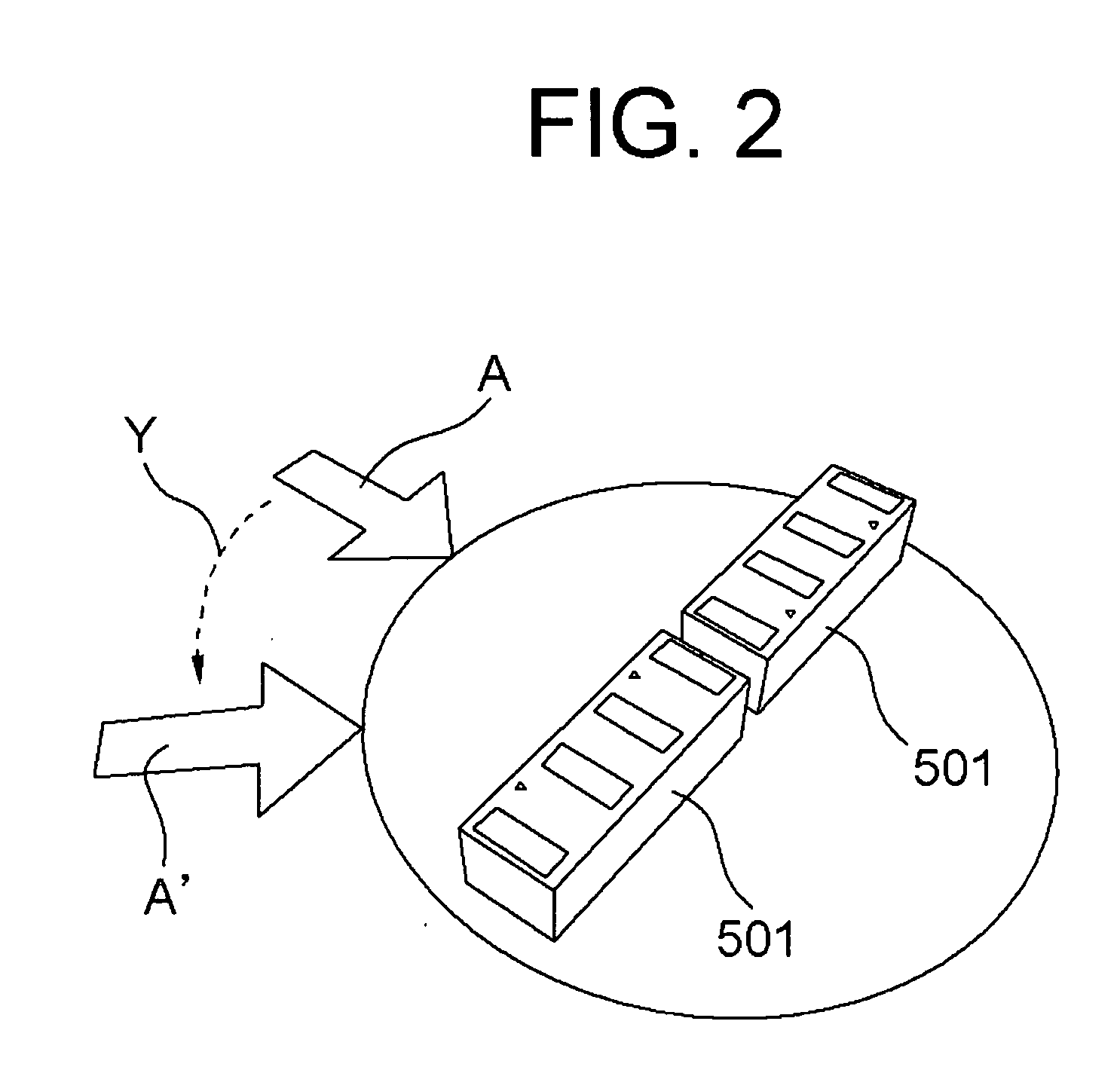
[0069]A first embodiment of the present invention will be described by referring to FIG. 8-FIG. 11. FIG. 8 and FIG. 9 are illustrations showing a schematic structure of the magnetic sensor according to the first embodiment, and FIG. 10 provides illustrations showing a state of the magnetic sensor in use. FIG. 11 is an illustration for describing facing directions of GMR chips.

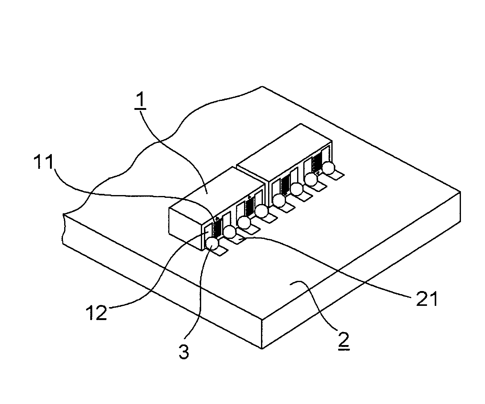
[0070]First, the magnetic sensor according to the embodiment comprises a GMR chip 1 (magnetic field detection chip) using, as an element for detecting a change in a magnetic field, a spin-valve type GMR element (giant magnetoresistive element) whose resistance value to be outputted changes in accordance with the direction of inputted magnetic field. Specifically, as shown in FIG. 8, the GMR chip 1 is substantially in a cuboid shape. A GMR element 11 having magnetization fixed in a prescribed direction so as to be able to detect the magnetic field in a prescribed direction and a pair of output terminals for outp...

second embodiment

[0081]Next, a second embodiment of the present invention will be described by referring to FIG. 12-FIG. 23. FIG. 12-FIG. 14 are illustrations showing the structure of the magnetic sensor according to this embodiment. FIG. 15-FIG. 20 are illustrations for describing modification examples of the magnetic sensor according to the embodiment. FIG. 21-FIG. 23 are illustrations for describing a method for manufacturing the magnetic sensor.

[0082]First, the magnetic sensor according to the second embodiment employs almost the same structure as the one shown in FIG. 8 described in the first embodiment. That is, GMR chips 101 and 102, each having two GMR elements formed thereon, are mounted on a substrate 2 so as to constitute the magnetic sensor with four GMR elements in total. Here, the two GMR chips 101, 102 are arranged side by side on the substrate 2 so that the GMR elements A, B, C, D formed on the respective GMR chips 101, 102 are arranged in a straight line form. Further, at this time,...


PUM


Abstract

To provide a magnetic sensor that can be reduced in size and cost. Provided is a magnetic sensor which comprises: a magnetic field detection chip having a magnetic field detection element for detecting a magnetic field and an output terminal for outputting an output signal from the magnetic field detection element; and a substrate that has the magnetic field detection chip mounted thereon, and has a connection terminal for being connected to the output terminal of the magnetic field detection chip that is formed on a mount face of the substrate. An output-terminal formed face of the magnetic field detection chip is arranged not to be in parallel to the mount face of the substrate. More specifically, the output-terminal formed face of the magnetic field detection chip is arranged almost vertical to the mount face of the substrate.

Description

BACKGROUND OF THE INVENTION[0001]1. Field of the Invention[0002]The present invention relates to a magnetic sensor capable of detecting changes in a magnetic field.[0003]2. Description of the Related Art[0004]A magnetic sensor capable of detecting changes in a magnetic field has been developed as a measuring device, and it is used for various applications such as a magnetic encoder, an open / close switch, an azimuth sensor, for example. Examples of such magnetic sensors are disclosed in Patent Documents 1 and 2 described below. The sensors depicted in those Patent Documents use GMR elements (giant magnetoresistive elements) as the elements for detecting the changes in the magnetic field. The GMR element is an element whose resistance value to be outputted changes in accordance with inputted magnetism. Thus, it is possible with the GMR element to measure a change in the detected magnetic field based on the outputted resistance values.[0005]As an example of a specific structure of a ma...

Claims


Application Information

Patent Timeline
Patent Type & Authority Applications(United States)
IPC IPC(8): G01R33/09G01R3/00
CPCG01R33/093B82Y25/00
Inventor KASAJIMA, TAMONSHOJI, SHIGERU
Owner SAE MAGNETICS (HK) LTD
Why Eureka
Try Eureka