Method and system for reducing via stub resonance

a technology of resonance and via, which is applied in the direction of high-frequency circuit adaptation, instrumentation, program control, etc., can solve the problems of difficult separation of connecting signal layers that are separated by many board layers, the inability to provide all components and connecting traces on one layer of the circuit board, and the thickness and cost of the board. achieve the effect of reducing the resonance of signal vias, increasing signal strength, and reducing the attenuation of vias

Inactive Publication Date:
View PDF21 Cites 63 Cited by
  • Summary
  • Abstract
  • Description
  • Claims
  • Application Information

AI Technical Summary

Benefits of technology

[0010]The present invention allows resonance in signal vias caused by via stubs to be significantly reduced, thus increasing signal strength and reducing attenuation in vias without having to perform elaborate and time consuming procedures such as back drilling via stubs.

Problems solved by technology

Since many applications such as servers and other complex devices have many connections and components, it is generally not possible to provide all the components and connecting traces on one layer of the circuit board.
The greater the number of layers used in a circuit board, the thicker and more expensive the board becomes.
Connecting signal layers that are separated by many board layers can be difficult.
However, this practice can be very expensive, since each via must be tailored to the exact length between the layers it is connecting.
High frequency signals commonly used in servers and other electronic devices can create problems in signal transmission when using circuit boards with vias due to parasitic effects.
One cause of poor signal quality is an impedance mismatch or discontinuity between via impedance and the impedance of the transmission line, which results in signal reflections.
Another cause of poor signal quality is resonance from via stubs, which may have a more significant effect on signal integrity than impedance mismatch at high frequencies.
A problem with the second practice of providing long vias is that a long unused portion of a long via, i.e. a via stub, may “dangle” and cause via stub resonance.
At high frequencies of signals, this stub of the via behaves as a transmission line and resonates, which can create some severe attenuation (loss) in the transmission signal if the stub resonance occurs in the frequency band of operation.
The longer the length of the via stub, the lower the resulting resonant frequency, and the greater the chance that the signals will be affected.
All the high speed circuits on the board can be routed on the higher layers of the board, allowing back drilling at a constant length for all vias; or back drilling can be performed at multiple different lengths based on particular signals (and causing more expense).
However, back drilling can be an expensive procedure and can reduce the manufacturing yield of circuit boards.

Method used


Image

  • Method and system for reducing via stub resonance
  • Method and system for reducing via stub resonance
  • Method and system for reducing via stub resonance

Examples


Embodiment Construction

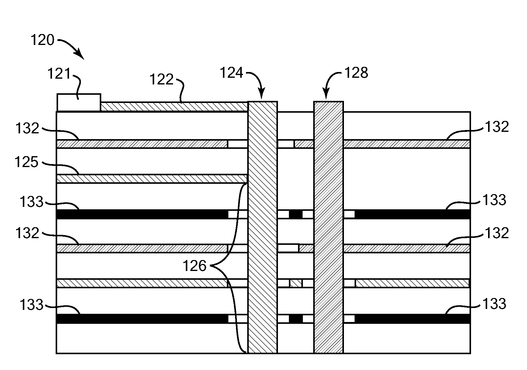
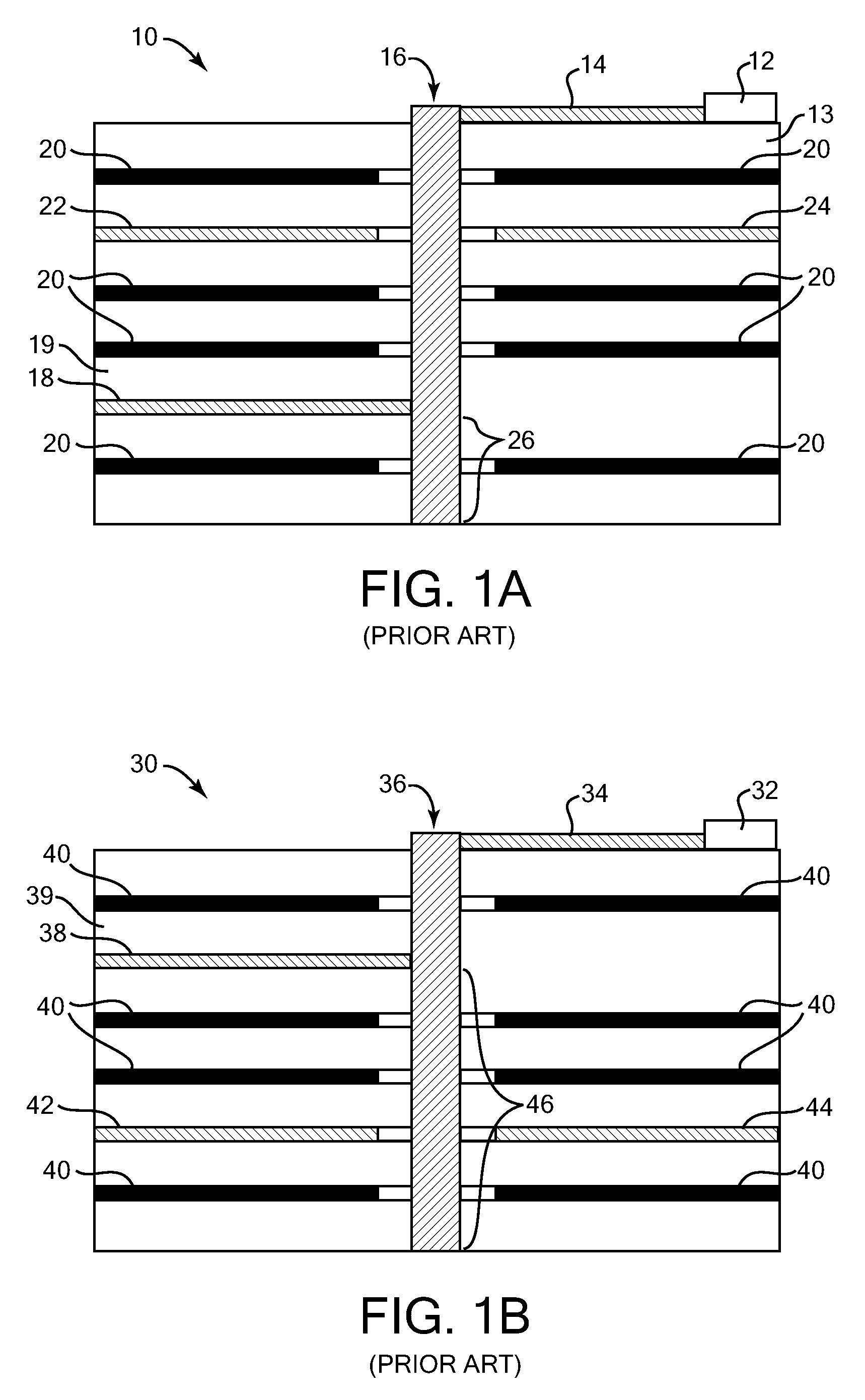
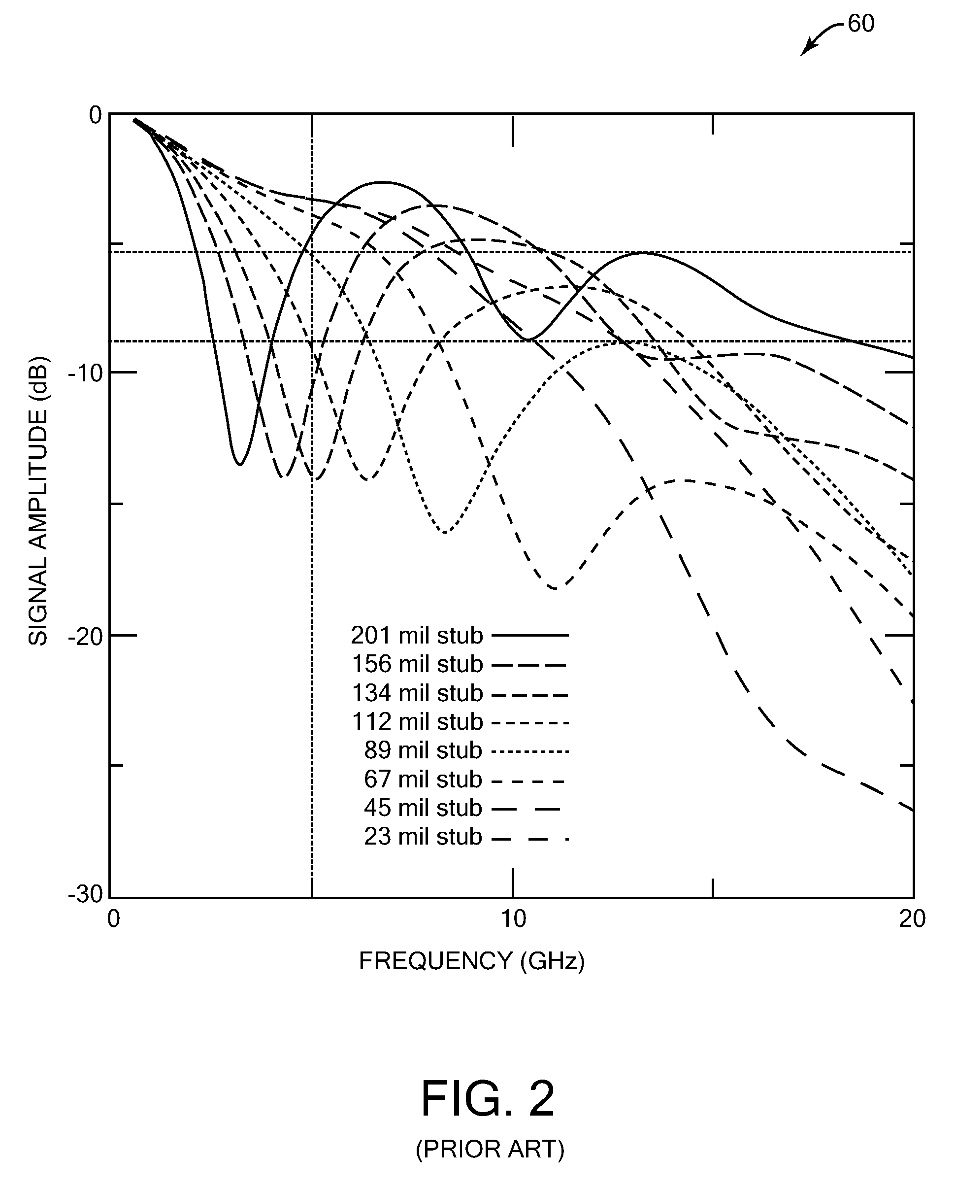
[0021]The present invention relates to printed circuit boards, and more particularly to via connections between layers in printed circuit boards. The following description is presented to enable one of ordinary skill in the art to make and use the invention and is provided in the context of a patent application and its requirements. Various modifications to the preferred embodiment and the generic principles and features described herein will be readily apparent to those skilled in the art. Thus, the present invention is not intended to be limited to the embodiment shown but is to be accorded the widest scope consistent with the principles and features described herein.

[0022]The present invention is mainly described in terms of particular systems provided in particular implementations. However, one of ordinary skill in the art will readily recognize that this method and system will operate effectively in other implementations. For example, the system implementations usable with the ...


PUM


Abstract

Reducing via stub resonance in printed circuit boards. In one aspect, a method for reducing via stub resonance in a circuit board includes determining that resonance exists for a signal to be transmitted through a signal via extending across a plurality of layers in the circuit board. The resonance is caused by a via stub of the signal via, the via stub extending past a layer connected to the signal via. A location is determined for a ground via to be placed relative to the signal via, the location of the ground via being determined based on reducing the resonance for the signal to be transmitted in the signal via.

Description

FIELD OF THE INVENTION[0001]The present invention relates to printed circuit boards, and more particularly to via connections between layers in printed circuit boards.BACKGROUND OF THE INVENTION[0002]Printed circuit boards are used extensively in computer systems and electronic devices. Circuit boards include many individual components that are interconnected by conductive traces etched on the printed circuit board. Since many applications such as servers and other complex devices have many connections and components, it is generally not possible to provide all the components and connecting traces on one layer of the circuit board. Thus, multiple layers are provided in the circuit board, each layer including its own traces and connected to other layers by signal vias (via transitions) that extend perpendicularly through different layers of the circuit board. A via is a copper (or other metal) barrel or cylinder which connects signal traces on one layer to signal traces on another la...

Claims


Application Information

Patent Timeline
Patent Type & Authority Applications(United States)
IPC IPC(8): G06F17/50H05K1/11
CPCG06F17/5068H05K1/0251H05K2201/09636H05K3/0005H05K3/429H05K1/115G06F30/39
Inventor MUTNURY, BHYRAV M.CASES, MOISESTUTEN, WALLACE G.MATOGLU, ERDEM
Why Eureka
Try Eureka