Photovoltaic cells

Inactive Publication Date: 2015-03-26
UNIV OF MANCHESTER
View PDF8 Cites 59 Cited by
  • Summary
  • Abstract
  • Description
  • Claims
  • Application Information

AI Technical Summary

Benefits of technology

[0052]If present, nanostructures can increase the signal strength of the cell (i.e. the photocurrent generated by the cell). Without wishing to be bound by theory, the increased signal strength arises due to two effects, firstly they act as a dopant for the graphene layer upon which they are placed, secondly they have a plasmonic effect. The dopant effect works largely as described above. A plasmonic effect is where the incident light interacts with the electrons in the metal nanostructure generating a dramatic enhancement in the local electric field. The effect is very localised. In systems in which the layers are not so thi

Problems solved by technology

It is sometimes called “insulating graphite” and it might be used in instances where graphene's high conductivity is a disadvantage (ultra-thin, high quality, insulating layers for nano-electronics, non-conductive, ultra-strong, composite materials).
However, there is still a large number of other layered materials whic

Method used


Image

  • Photovoltaic cells
  • Photovoltaic cells
  • Photovoltaic cells

Examples


example 1

Preparation of and Photovoltaic Ability of a Graphene / WS2 / Graphene Device

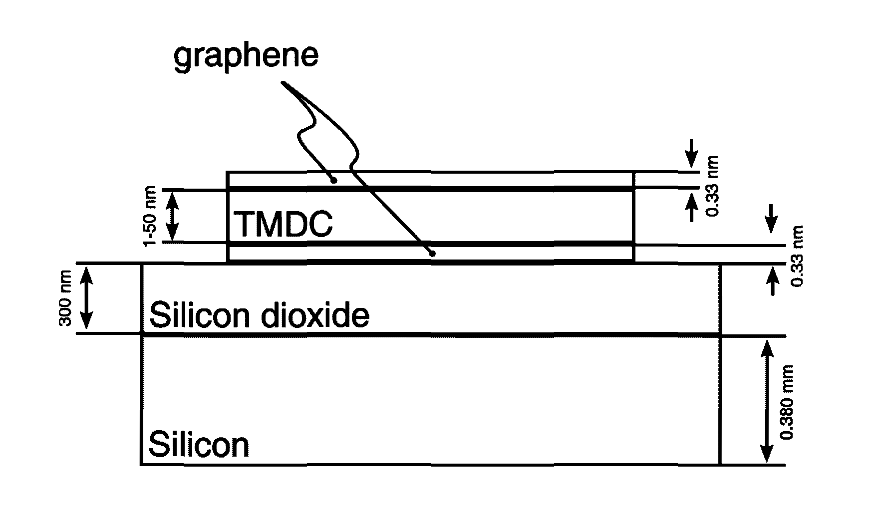
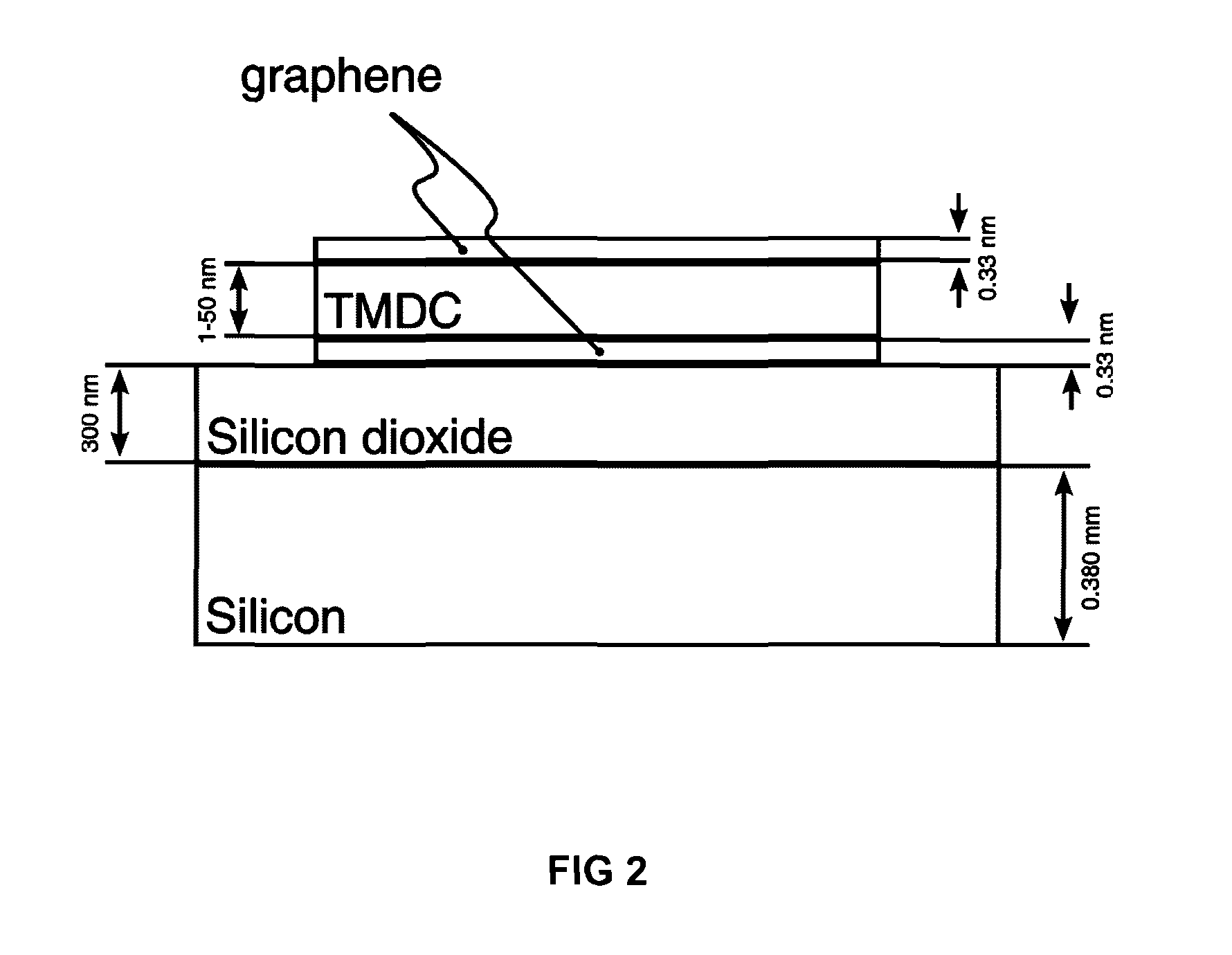
[0182]The experiments described in the following sections demonstrate a beneficial combination of the properties of graphene and WS2: WS2 as a good photoactive material and graphene as a good transparent electrode. Using a graphene / WS2 / graphene stack with appropriately positioned Fermi levels and simply doping the two graphene layers differently (either by electrostatic gating or chemical methods), leads to large photocurrent. The layered nature of our structures means it is possible to fabricate large area light harvesting devices. Without illumination, such devices act as tunnelling transistors.

[0183]Devices comprising three principal layers, top and bottom graphene electrode layers (we tested both micromechanically cleaved and CVD-grown graphene) sandwiching a photoactive WS2 layer, were prepared. The left hand panel in FIG. 1 shows an optical image of a device according to the invention. In the fabrication ...

example 2

Preparation of a Device of the Invention Using Solution Processed Materials

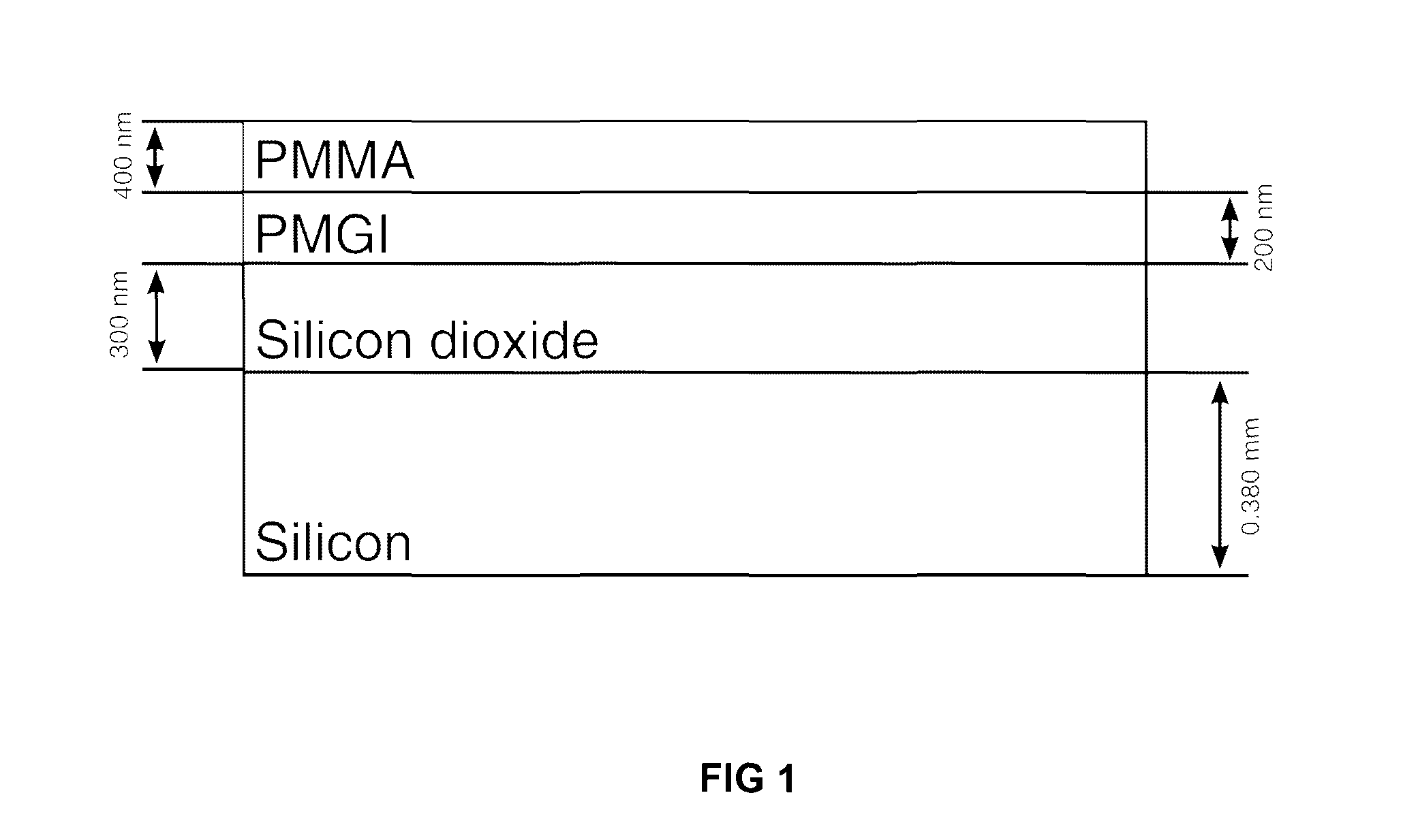
[0212]An alternative exemplary method of preparing the devices, cells and heterostructures according to the invention is as follows.[0213]1. Metal electrodes (Cr / Au (5 / 50 nm) in our case) are patterned onto a substrate (in this case silicon / silicon dioxide).[0214]2. A WS2 film is prepared as follows.[0215]a. WS2 powder is put into a 35% ethanol / water mixture and placed in an ultrasonic bath for 5 days to break up the WS2 crystals to few layer nanoplatlets which form a suspension.[0216]b. The suspension is filtered through a cellulose membrane and a film is left, attached to the filter.[0217]c. By dipping the membrane in water, a thin film (˜50 nm thick) delaminates from the WS2 film and is left floating on the water's surface.[0218]3. The membrane can be ‘fished’ from the water with the gold patterned substrate so that the WS2 film covers many metal electrodes.[0219]4. CVD graphene can then be transferred as ...

example 3

Preparation of a Flexible Device

[0221]A device as prepared in Example 1 was transferred to a PET (poly(ethylene terephthalate)) substrate and subjected to strain. As the device was put under strain, it's performance as a transistor was measured and it was found that there was no change of the current with a strain of up to about 5%. It was also shown that it is still possible to modulate the current when the device is under strain.

[0222]After it was subjected to strain, the photovoltaic properties of the device were tested as for the Si / SiO2 device described above.

[0223]The inset of FIG. 7 shows the photocurrent of the flexible device (inset, as crossed squares) after it has been placed under strain measured with a 1.95 eV laser as a function of intensity and follows a sublinear dependence.

[0224]In general, the EQE in our devices on Si / SiO2 substrate is somewhat higher in comparison with the flexible PET devices due to multiple reflections in SiO2 which effectively works as a cavity...


PUM


Abstract

This invention relates to cells and devices for harvesting light. Specifically the cell comprises at least one electrode which comprises graphene or modified graphene and layer of a transition metal dichalcogenide in a vertical heterostructure. The cell may be part of a light harvesting device. The invention also relates to materials and methods for making such cells and devices.

Description

[0001]This invention relates to cells and devices for harvesting light. Specifically the cell comprises at least one electrode which comprises graphene or modified graphene and layer of a transition metal dichalcogenide in a vertical heterostructure. The cell may be part of a light harvesting device. The invention also relates to materials and methods for making such cells and devices.BACKGROUND[0002]Graphene is a two-dimensional allotrope of carbon, in which a planar sheet of sp2 hybridised carbon atoms is arranged in a ‘honeycomb pattern’ of tessellated hexagons. Essentially graphene is a single layer of graphite. Graphene is a semi metal with high room temperature charge carrier mobility. It is stable in ambient conditions and its electronic properties can be controlled through application of an electric field as with traditional silicon transistors (K. S, Novoselov, A. K. Geim, S. V. Morozov, D. Jiang, Y. Zhang, S. V. Dubonos, I.V. Grigorieva and A. A. Firsov, “Electric field Ef...

Claims


Application Information

Patent Timeline
IPC IPC(8): H01L31/0352H01L31/18H01L31/0224
CPCH01L31/035209H01L31/18H01L31/186H01L31/022433B82Y30/00H01L31/022466H01L31/1884Y02E10/50H01L31/032H01L31/022425
Inventor NOVOSELOV, KONSTANTINBRITNELL, LIAM
Owner UNIV OF MANCHESTER
Why Eureka
Try Eureka