Multifunction organic diode and matrix panel thereof

a multi-functional, organic diode technology, applied in the direction of instruments, static indicating devices, thermoelectric devices, etc., can solve the problem of device size limitation by wafer size, and achieve the effects of high internal quantum efficiency, good carrier injection balance, and high exciton generation efficiency

Inactive Publication Date: 2009-02-26
UNIVERSITY OF TOYAMA
View PDF3 Cites 15 Cited by
  • Summary
  • Abstract
  • Description
  • Claims
  • Application Information

AI Technical Summary

Benefits of technology

[0016]When the functions of an organic EL device and an organic photo sensing device is intended to be realized by a single device, it is required from a view point of the light emission device that a visible light emission from the organic material should not be absorbed by the organic material itself, and furthermore that it has a good carrier injection balance which is a feature of a typical organic EL device, a high exciton generation efficiency, and a high internal quantum efficiency. Also from a view point of a photo sensing device it should meet those requirements which are that sufficiently high optical absorption can be attained for an incident radiation with wavelength satisfying the optical absorption band of the organic material itself, that the internal quantum efficiency is high enough for a number of electron-hole pair generated for each incident photon being equal to one and that a carrier transport in the material is efficient enough for the generated carrier to be swept out without being trapped by a band offset, a carrier trap, and the like.

Problems solved by technology

As drawback of the Si semiconductor, there are, however problems such as that it is not light emitting, that the device size is limited by a wafer size, and that it is heavy.

Method used


Image

  • Multifunction organic diode and matrix panel thereof
  • Multifunction organic diode and matrix panel thereof
  • Multifunction organic diode and matrix panel thereof

Examples


embodiments

[0096]Embodiments in accordance with the present invention will be described in the following.

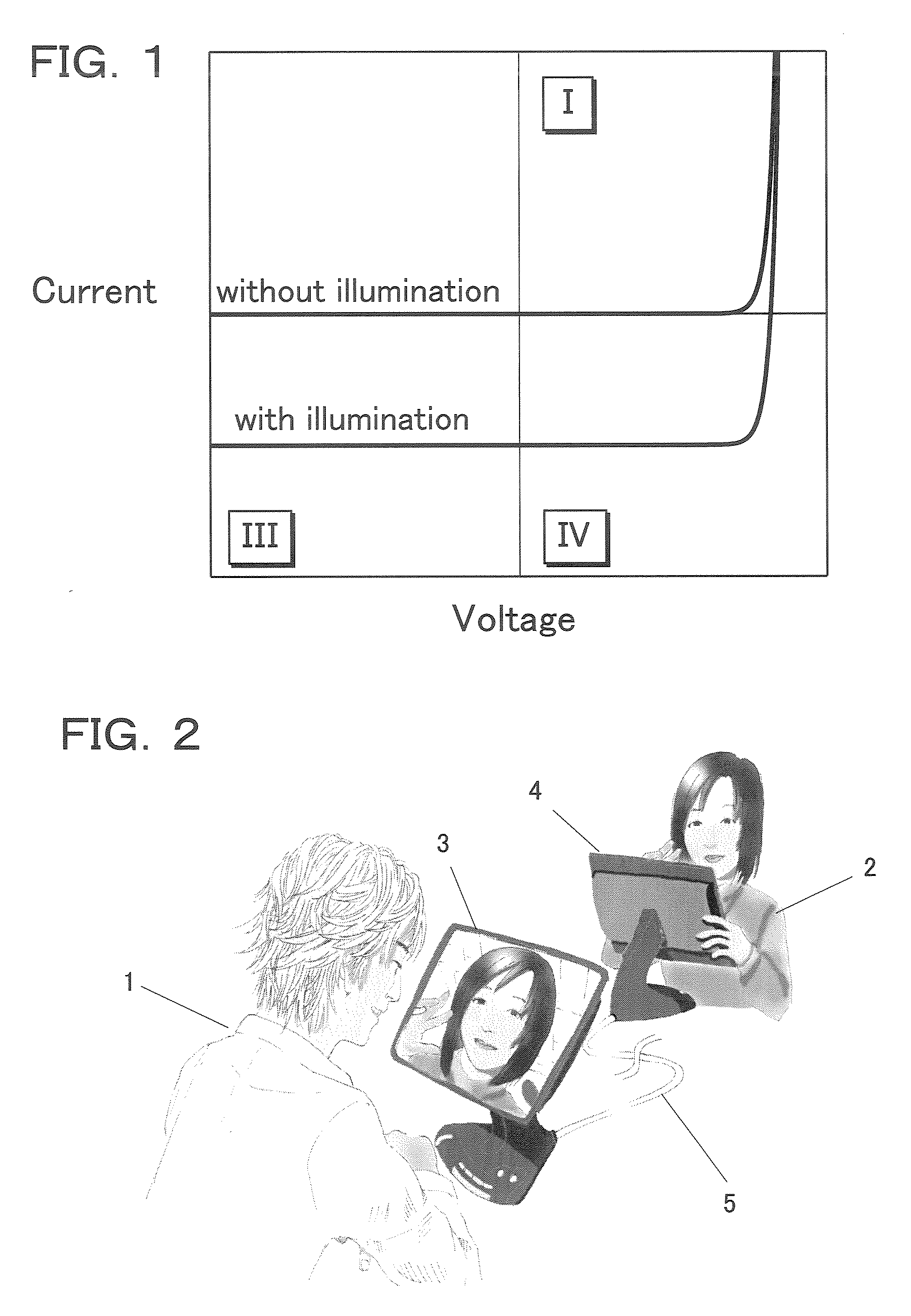
[0097]FIG. 2 shows an example of a composite function television as an application example implemented by the present invention.

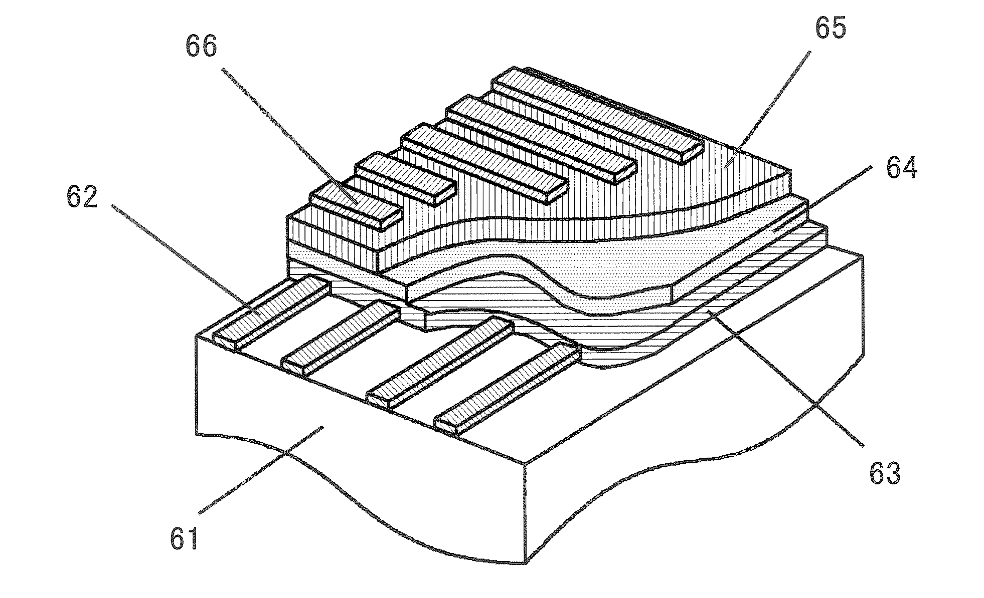
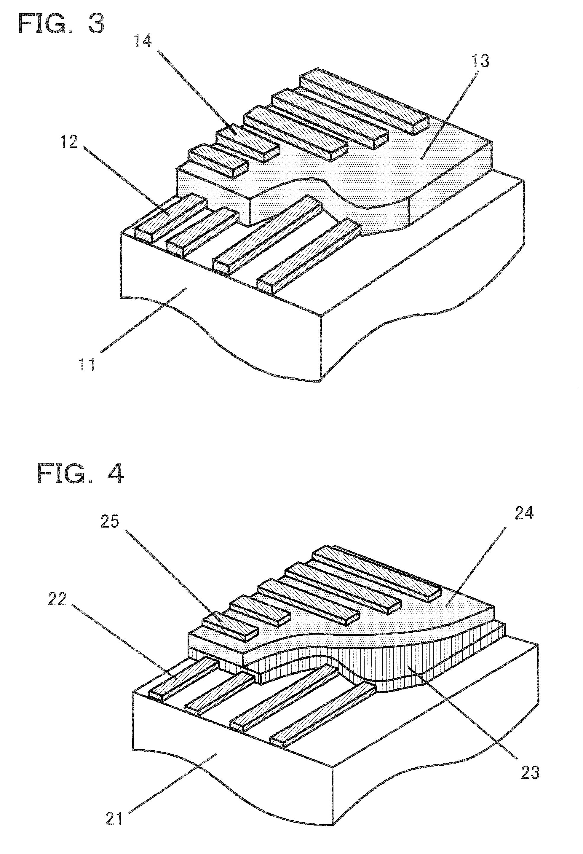
[0098]In this figure, 1 is a first observer, 2 is a second observer, 3 is a first display, 4 is a second display, and 5 is a cable.

[0099]By alternately performing display and read-in of image information within a frame period with the first display 3 and the second display 4, images of the facing observers are displayed during the display period and read-in through the display during the read-in period of information. Here the image display part / image read-in part performs image display and image read-in, respectively, corresponding to R(red), G(green) and B(blue). Alternatively, the image display part and the image read-in part can be fabricated in a separate position on the surface of the same display. In this case, the image display and the image read-in can be ...


PUM


Abstract

Disclosed is organic diode which is capable of light emitting display by an organic EL display, image sensing by a organic photodiode and power generation by an organic solar cell. Also disclosed is a matrix panel of such a multifunction organic diode. Specifically disclosed is a multifunction organic diode comprising a first electrode (12) formed on a substrate (11), an organic thin film (13) formed on the first electrode (12) and having both light emitting and photoconductive properties, and a second electrode (14) formed on the organic thin film (13).

Description

TECHNICAL FIELD[0001]The present invention relates to a multifunction organic diode and a matrix panel thereof, and more particularly, to the multifunction organic diode and the matrix panel thereof showing functions as an organic EL, organic photodiode and organic solar cell.BACKGROUND ART[0002]Conventionally, a main role of devices supporting electronics and information apparatus has been played by a Si semiconductor, and by means of the integrated circuit thereof, development of numerous products such as an electronic apparatus, a computer, a communication apparatus, and a domestic product has been achieved. As drawback of the Si semiconductor, there are, however problems such as that it is not light emitting, that the device size is limited by a wafer size, and that it is heavy. As a result, a compound semiconductor has been developed as a light emitting device, and an amorphous or polycrystal Si semiconductor has been developed as a large area panel.[0003]Due to this situation,...

Claims


Application Information

Patent Timeline
Patent Type & Authority Applications(United States)
IPC IPC(8): H01L51/00
CPCG09G3/2003H01L51/5012G09G3/3241G09G3/325G09G3/3258G09G2300/0417H01L27/301H01L27/307H01L27/3244H01L27/3281H01L51/0053H01L51/0062H01L51/0078H01L51/0081H01L51/424G09G3/3216H10K39/10H10K39/32H10K59/12H10K59/17H10K85/621H10K85/649H10K85/311H10K85/324H10K30/20H10K50/11
Inventor OKADA, HIROYUKINAKA, SHIGEKIONNAGAWA, HIROYOSHI
Owner UNIVERSITY OF TOYAMA
Why Eureka
Try Eureka