Stack package and method of fabricating the same

a technology of stacking and stacking, which is applied in the direction of semiconductor devices, semiconductor/solid-state device details, electrical apparatus, etc., can solve the problems of increasing the height of the horizontal package, complex manufacturing process, and considerable heat generated during operation, so as to reduce the height of the stacking. , the effect of reducing the heigh

Inactive Publication Date: 2009-02-26
SAMSUNG ELECTRONICS CO LTD
View PDF6 Cites 15 Cited by
  • Summary
  • Abstract
  • Description
  • Claims
  • Application Information

AI Technical Summary

Benefits of technology

[0009]The present invention provides a stack package whose height can be reduced and which can be easily fabricated. The present invention also provides a method of fabricating a stack package whose height can be reduced and which can be easily fabricated. The present invention further provides a stack package which can provide high heat dissipation efficiency, can be manufactured with a reduced height, and can be simply fabricated, and a method of fabricating the stack package.

Problems solved by technology

However, since the semiconductor chip is connected to the package substrate by wire bonding, a molding process must be performed to protect the wires, thereby increasing the height of the horizontal package and leading to a complex manufacturing process.
Meanwhile, as semiconductor chips have recently been highly integrated into a small area to achieve high performance, considerable heat is generated during operation.
The heat generated in the semiconductor chips significantly increases the temperature of the package, thereby increasing the risk of malfunction.

Method used


Image

  • Stack package and method of fabricating the same
  • Stack package and method of fabricating the same
  • Stack package and method of fabricating the same

Examples


Embodiment Construction

[0014]The present invention will now be described more fully with reference to the accompanying drawings, in which exemplary embodiments of the invention are shown. The invention may, however, be embodied in different forms and should not be construed as limited to the embodiments set forth herein. Rather, these embodiments are provided so that this disclosure will be thorough and complete, and will fully convey the scope of the invention to those skilled in the art. In the drawings, the thicknesses of layers and regions are exaggerated for clarity. Like reference numerals refer to like elements throughout.

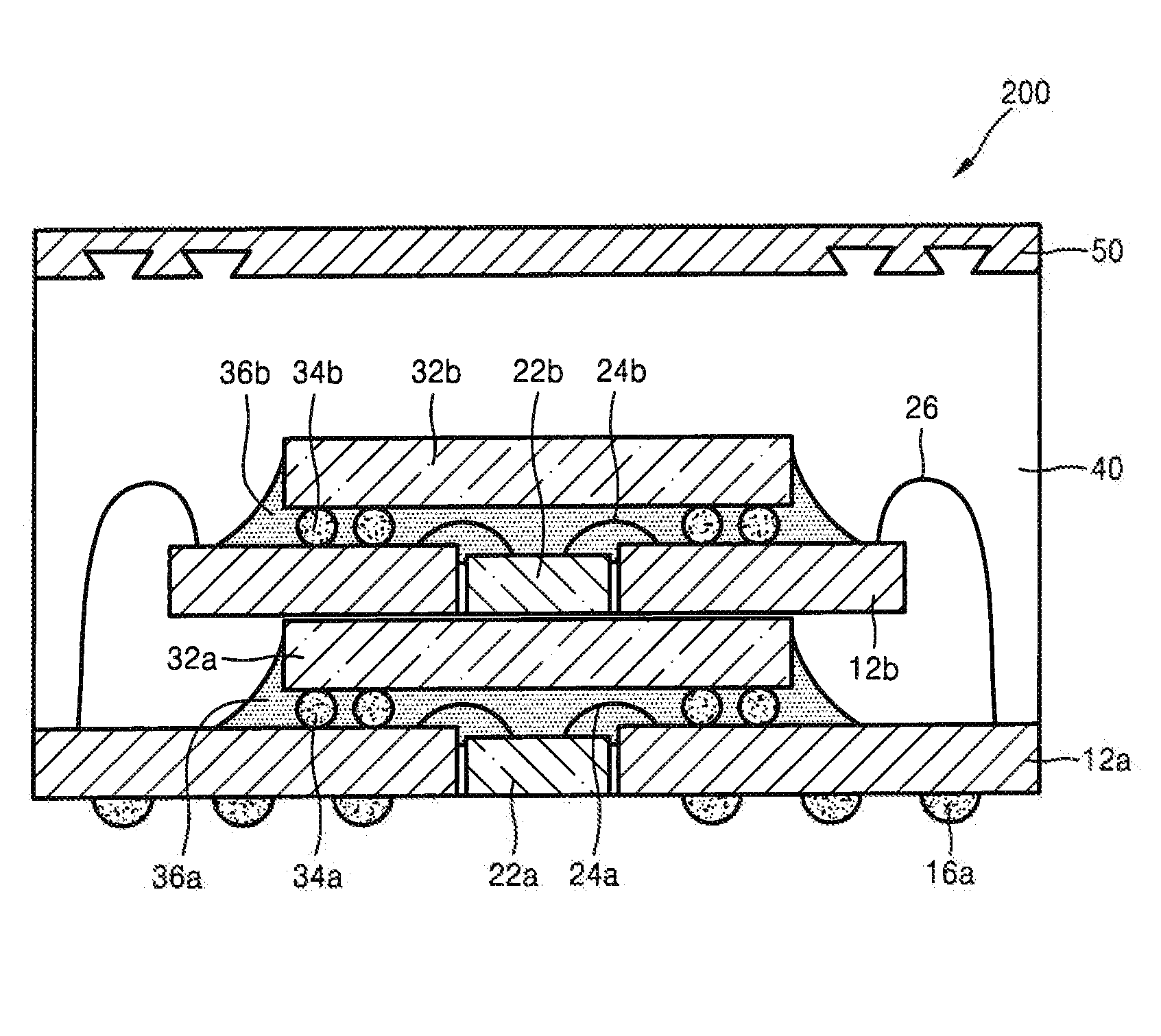
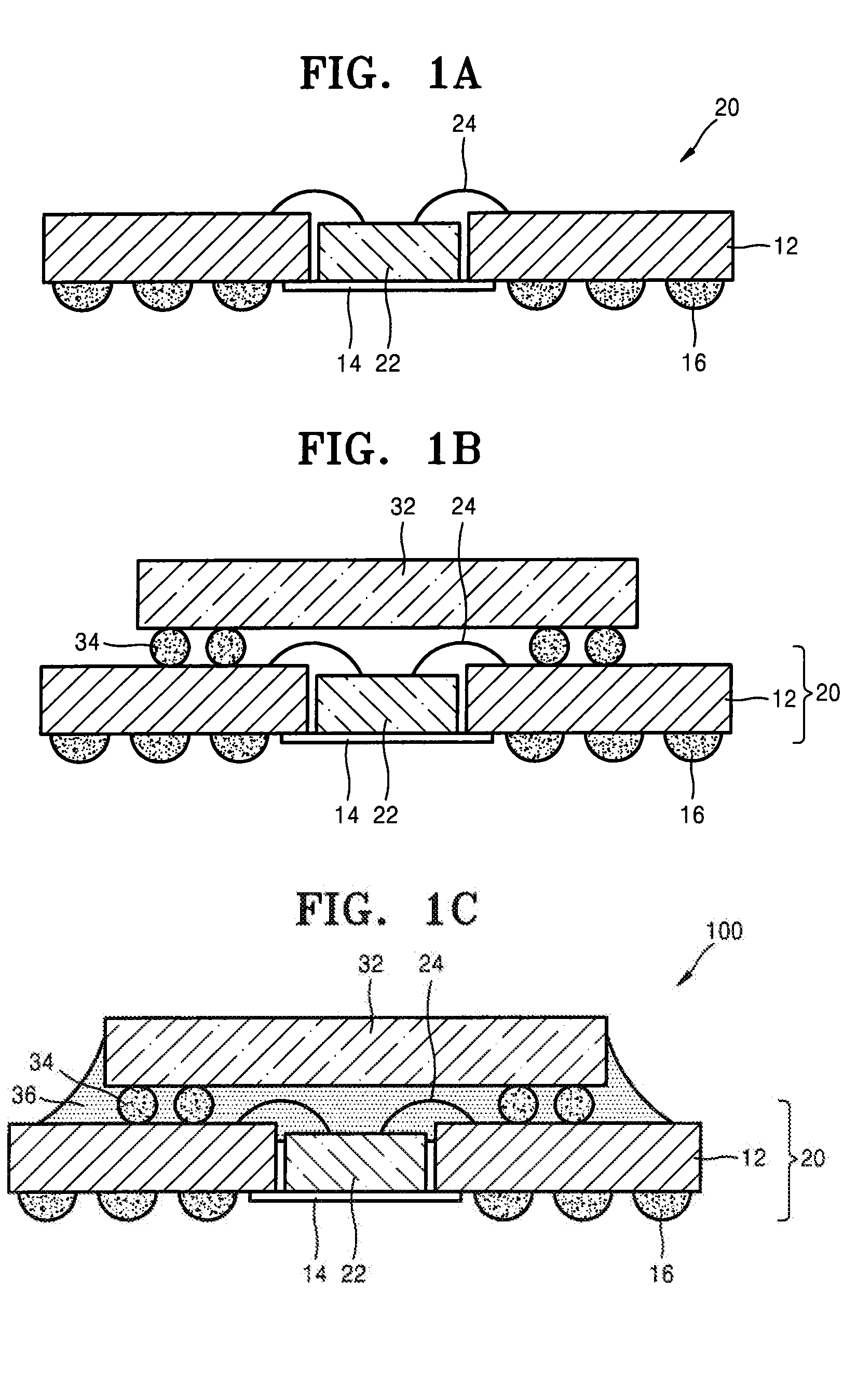
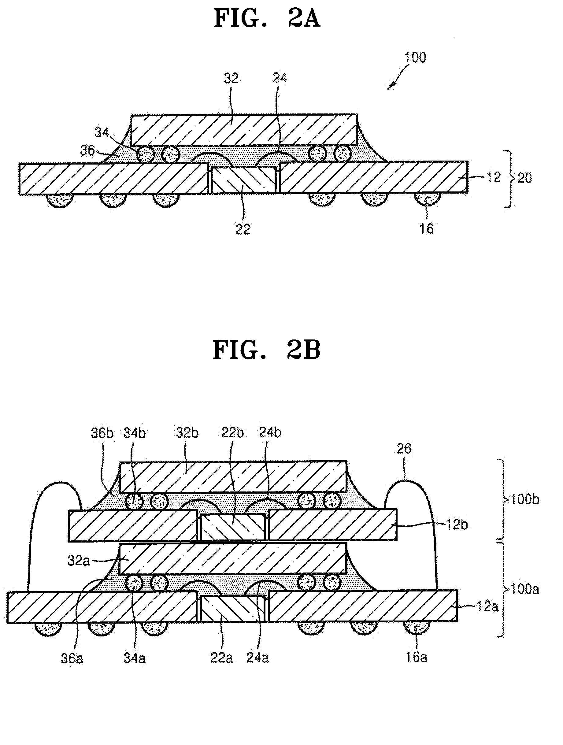
[0015]FIGS. 1A through 1C are cross-sectional views illustrating a method of fabricating a stack package 100 according to an embodiment of the present invention. The structure of the stack package 100 will now be explained first with reference to FIG. 1C.

[0016]Referring to FIG. 1C, the stack package 100 includes a horizontal package 20 including a first semiconductor chip 22, and ...


PUM


Abstract

Provided is a stack package comprising: a substrate comprising a cavity; a first semiconductor chip disposed in the cavity; and a second semiconductor chip stacked on the substrate and electrically connected to the substrate by a plurality of conductive external terminals such as conductive bumps. Since both a horizontal packaging method using bonding wires and a flip-chip packaging method are used and the bonding wires of the horizontal package and the conductive external terminals for the flip-chip bonding are formed on substantially the same plane, the total height of the stack package is reduced.

Description

CROSS-REFERENCE TO RELATED PATENT APPLICATION[0001]This application claims priority under 35 USC § 119 to Korean Patent Application No. 10-2007-0001689, filed on Jan. 5, 2007 in the Korean Intellectual Property Office, the contents of which are incorporated herein in their entirety by reference.BACKGROUND[0002]1. Technical Field[0003]The present invention relates to a semiconductor package, and more particularly, to a stack package in which a plurality of semiconductor chips are stacked.[0004]2. Description of the Related Art[0005]With the recent development of smaller and higher performance electrical and electronic devices, higher capacity semiconductor modules are required. One solution to meet the demand for higher capacity semiconductor modules is to use semiconductor packaging technology to increase the capacity of individual semiconductor packages. Accordingly, multi-chip package (MCP) technology, which mounts a plurality of chips in a single package, has recently been develo...

Claims


Application Information

Patent Timeline
Patent Type & Authority Applications(United States)
IPC IPC(8): H01L23/02
CPCH01L21/6835H01L2924/1815H01L24/16H01L24/48H01L25/03H01L25/0657H01L2224/16225H01L2224/48091H01L2224/48227H01L2225/0651H01L2225/06517H01L2225/06589H01L2924/15153H01L2924/1517H01L2924/15311H01L2924/15331H01L2924/18165H01L2924/18301H01L2924/19107H01L23/4334H01L2924/00014H01L2924/181H01L2924/00012H01L2224/45099H01L2224/45015H01L2924/207H01L23/48H01L23/12
Inventor NAM, TAE-DUKPARK, HEE-JINOH, JEONG-JOON
Owner SAMSUNG ELECTRONICS CO LTD
Why Eureka
Try Eureka