Pattern forming apparatus and pattern forming method

a technology of pattern forming and pattern forming, which is applied in the direction of electrographic process, instruments, optical elements, etc., can solve the problems of limiting the increase of resolution and productivity, the need for huge and high-cost manufacturing equipment, and the inability to meet the requirements of large-scale production, etc., to achieve higher resolution, higher positional accuracy, and high thickness

Inactive Publication Date: 2009-02-26
KK TOSHIBA
View PDF9 Cites 5 Cited by
  • Summary
  • Abstract
  • Description
  • Claims
  • Application Information

AI Technical Summary

Benefits of technology

[0016]An object of the present invention is to provide a pattern forming apparatus and a pattern forming method capable of forming a pattern of higher thickness with higher resolution and higher positional accuracy.
[0017]In addition, another object of the present invention is to provide a pattern forming apparatus and a pattern forming method capable of shortening processing time for development thereby to improve operation rate of the apparatus.

Problems solved by technology

However, while this photolithography asks higher resolution or greater performance, it needs huge and highly-expensive manufacturing equipment and its manufacturing cost becomes higher according to the resolution.
Meanwhile, in the field of manufacturing a semiconductor device, an image display and the like, there are increasing demands for performance improvement and lower costs, and it is difficult for the above-mentioned photolithography to meet these needs.
However, there are limits in increasing the resolution and productivity.
However, this need cannot be satisfied by the above-mentioned electrophotographic system.
This is because the resolution of the writing optical system is about 1200 dpi at most, which is not enough to assure higher resolution and higher positional accuracy.
In addition, there is a problem that the wide wiring optical system for recent larger-sized displays cannot yet be realized.
However, after the inventors of the present application carried out experiments and studied intensively, they found the following substantial problems of this method.
First, the developed image with use of liquid toner often has a film thickness of 1 μm or less, and is not suitable for thick film formation such as phosphor layer and color filter of a display.
In addition, when a corona charger is used to transfer the developed image onto the glass plate, corona charge propagates on the glass surface and is leaked, which tends to cause unstable transfer performance.
In addition, a space charge tends to be stored inside the glass and it is difficult to form a transfer electric field that is stronger than this space charge in the corona transfer.
Further, this problem is exacerbated after a first color developed image is transferred, which makes it more difficult to transfer the second and third color developed images onto the glass plate.
Further, in the method of using an electrostatic printing plate, it is difficult to develop image of plural colors at the same time, which makes it necessary to perform development and transferring process for each color.
This presents problems of longer processing time for one-time print and lower operation rate.

Method used


Image

  • Pattern forming apparatus and pattern forming method
  • Pattern forming apparatus and pattern forming method
  • Pattern forming apparatus and pattern forming method

Examples


first embodiment

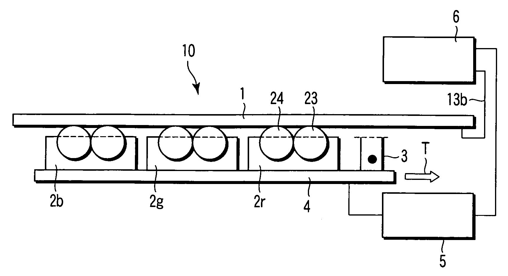
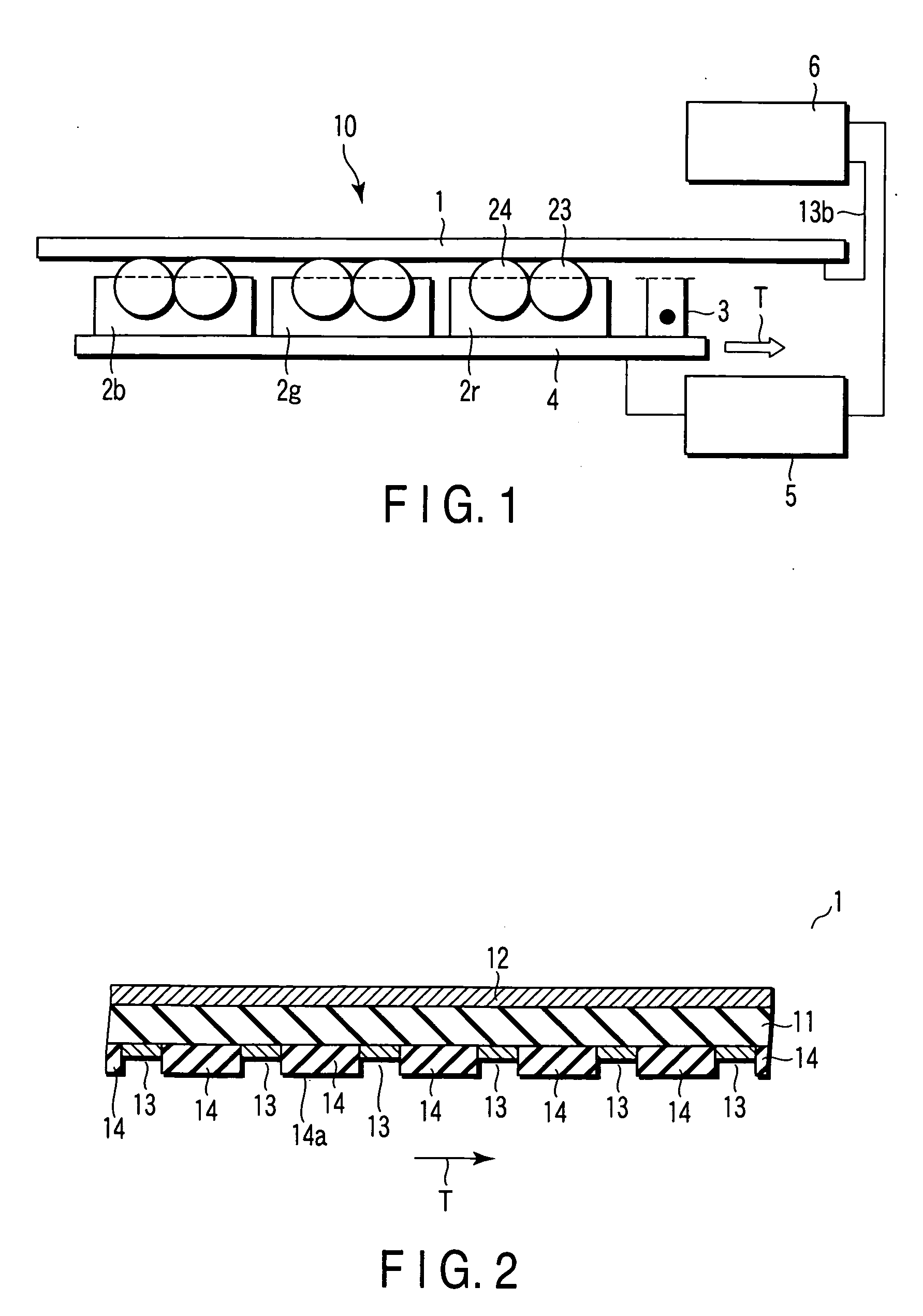
[0042]FIG. 1 schematically illustrates the structure of substantial parts of a pattern forming apparatus 10 according to the present invention. The pattern forming apparatus 10 described here is, for example, an apparatus for forming a color filter and a phosphor layer on the inner surface of a display panel of a flat panel display.

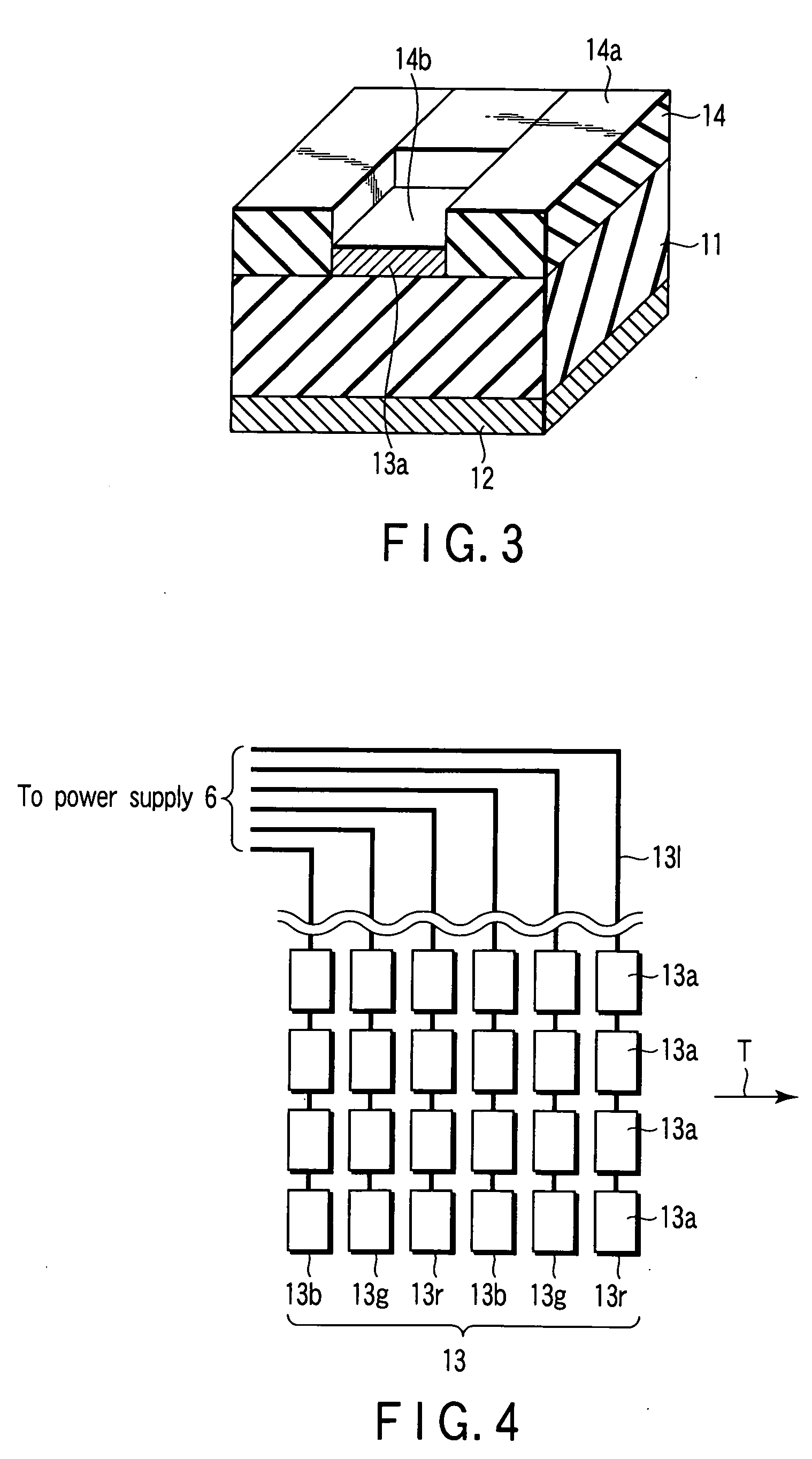
[0043]The pattern forming apparatus 10 has a flat depressed plate 1 as a plate of this invention; plural developing devices 2r, 2g and 2b (which are sometimes collectively called developing devices 2 below), arranged below the depressed plate 1 in the figure and closely opposed to the depressed plate 1, for supplying the depressed plate 1 with liquid developers of colors (r: red, g: green, b: blue) to perform development; a charging device 3 for charging a surface 14a of a high-resistance layer 14 (which is described later) of the depressed plate 1 at a predetermined potential; and a stage 4 holding the charging device 3 and the plural developing devices ...

third embodiment

[0104]Next description is given about a pattern forming apparatus 70 according to the present invention with reference to FIG. 18.

second embodiment

[0105]The pattern forming apparatus 70 has a drum-shaped depressed plate 1, a charging device 3, developing devices 2r, 2g and 2b and a cleaner 71 which are arranged fixedly around the depressed plate 1. The depressed plate 1 is made of a conductive material such as aluminum, stainless steel or the like, and the structural elements shown in FIG. 2 are deposited on the surface of the depressed plate 1. Otherwise, the conductive drum may be used as a common electrode 12 and other structural elements may be formed into separate insulating sheets and wound around the conductive drum. The power supply 6 has embedded therein a controller according to the above-described first or second embodiment, and the controller receives, as positional information 51, a signal from an encoder 72 provided at the rotational axis of the depressed plate 1.

[0106]Then, around the depressed plate 1, between the blue developing device 2b and the cleaner 71, a transfer target medium 31 is arranged closely faci...


PUM


Abstract

A pattern forming apparatus includes a depressed plate holding patterns by developers, a charging device for charging the depressed plate, a developing device for developing a red pattern, a developing device for developing a green pattern, a developing device for developing a blue pattern, and a stage for holding the charging device and the developing devices and moving them relative to the depressed plate. The charging device, the red developing device, the green developing device and the blue developing device pass along the depressed plate sequentially to perform the charging process, the red developing process, the green developing process and the blue developing process simultaneously.

Description

CROSS REFERENCE TO RELATED APPLICATIONS[0001]This is a Continuation Application of PCT Application No. PCT / JP2007 / 053790, filed Feb. 28, 2007, which was published under PCT Article 21(2) in Japanese.[0002]This application is based upon and claims the benefit of priority from prior Japanese Patent Application No. 2006-056502, filed Mar. 2, 2006, the entire contents of which are incorporated herein by reference.BACKGROUND OF THE INVENTION[0003]1. Field of the Invention[0004]The present invention relates to a pattern forming apparatus and a pattern forming method used in, for example, manufacturing a flat panel display, wiring board, IC tag and the like.[0005]2. Description of the Related Art[0006]Conventionally, photolithography plays a main role in forming a fine pattern on a base material surface. However, while this photolithography asks higher resolution or greater performance, it needs huge and highly-expensive manufacturing equipment and its manufacturing cost becomes higher acc...

Claims


Application Information

Patent Timeline
Patent Type & Authority Applications(United States)
IPC IPC(8): G03G13/04G03G15/10
CPCG02B5/201G03G15/344H05K2203/0517H05K3/1266H05K3/207G03G2215/0658B41J2/385
Inventor ISHII, KOICHIHOSOYA, MASAHIRO
Owner KK TOSHIBA
Why Eureka
Try Eureka