

Electronic Assemblies Without Solder and Methods for their Manufacture
- Summary
- Abstract
- Description
- Claims
- Application Information
AI Technical Summary
Benefits of technology
Problems solved by technology
Method used
Image

Examples
Embodiment Construction
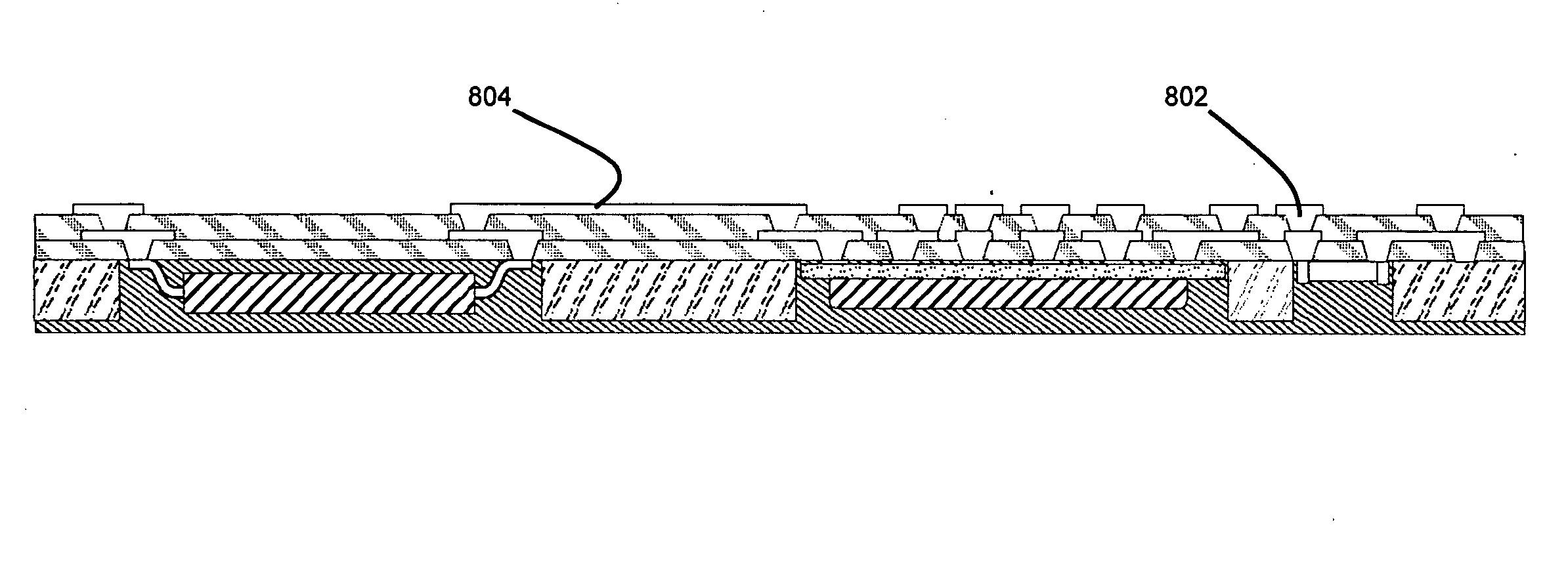
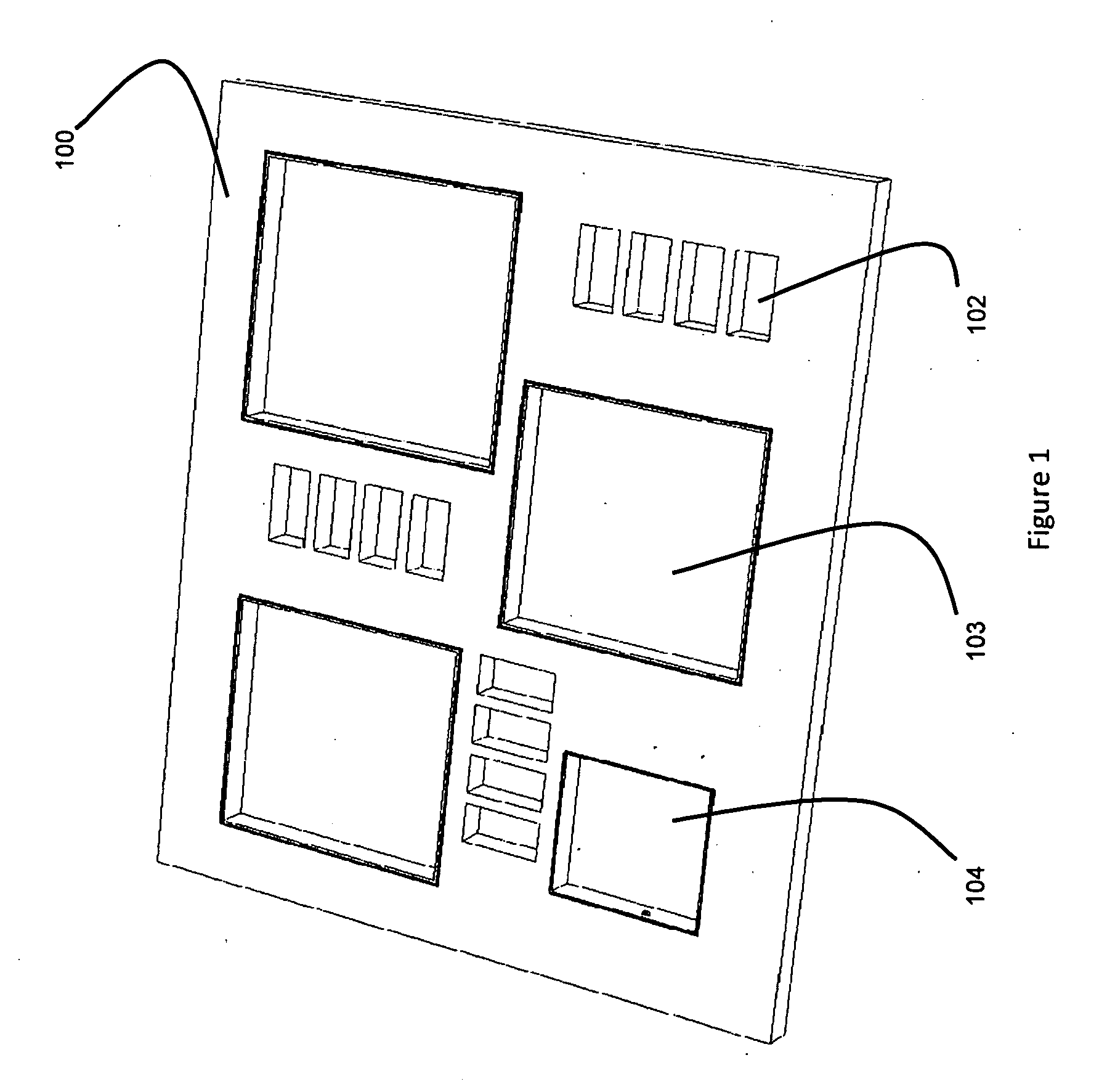
[0030]FIG. 1 shows a frame 100 with apertures 102, 103, and 104 into which electrical components may be inserted. The frame 100 may be continuous, sectioned, in multiple discrete pieces or temporarily attached to other pieces of frame in anticipation of creating a finished structure which will have flexible areas in the completed assembly to allow for subsequent folding or bending of the assembly. FIG. 2 shows electrical components (for example discrete component 202, land grid array component 203, and gull wing component 204) in position over respective apertures 102, 103, and 104 of frame 100. Frame 100 sits on a substrate 206 which may be either temporarily or permanently attached to frame 100.
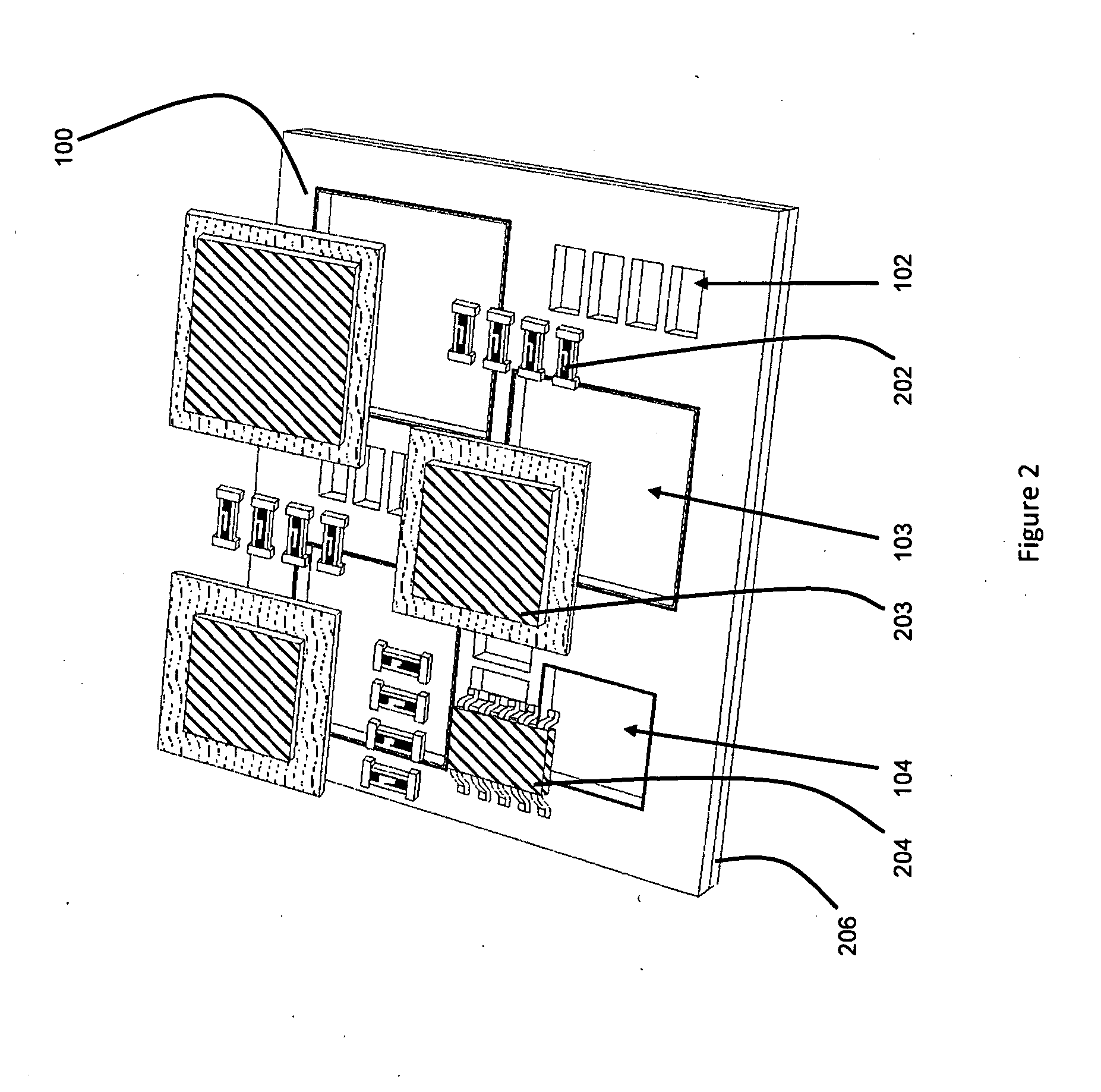
[0031]FIG. 3 shows a section of frame 100 situated on substrate 206 with components 202, 203, and 204 inserted into respective apertures 102, 103, and 104 and attached to substrate 206.
[0032]FIG. 4 shows subassembly 400, including frame 100 and substrate 206, with electrically insulating ma...
PUM
| Property | Measurement | Unit |
|---|---|---|
| Electrical conductivity | aaaaa | aaaaa |
| Flexibility | aaaaa | aaaaa |
| Electrical conductor | aaaaa | aaaaa |
Abstract
Description
Claims
Application Information