Optical semiconductor device and manufacturing method therefor

a technology of optical semiconductor and manufacturing method, which is applied in the direction of semiconductor/solid-state device manufacturing, semiconductor/semiconductor devices, electrical apparatus, etc., can solve the problems of increasing the density of threading dislocation of nitride semiconductor thin films, and achieve the effect of reducing threading dislocation and improving the maximum power of ultraviolet leds

Inactive Publication Date: 2009-03-05
RIKEN
View PDF7 Cites 21 Cited by
  • Summary
  • Abstract
  • Description
  • Claims
  • Application Information

AI Technical Summary

Benefits of technology

[0016]According to the present invention, a high-quality AlGaN buffer for an ultraviolet LED can be produced. The pulsed supply of TMAl enables the group III polarity to be achieved. The pulsed supply of TMAl advantageously re

Problems solved by technology

However, in manufacturing a semiconductor light emitting device using a nitride semiconductor, it is required to use a sapphire substrate, for example, as an epitaxial growth substrate, because it is difficult, or expensive even if possible, to produce a high-quality and large-area epitaxial growth substrate of a nitride semiconduct

Method used


Image

  • Optical semiconductor device and manufacturing method therefor
  • Optical semiconductor device and manufacturing method therefor
  • Optical semiconductor device and manufacturing method therefor

Examples


Embodiment Construction

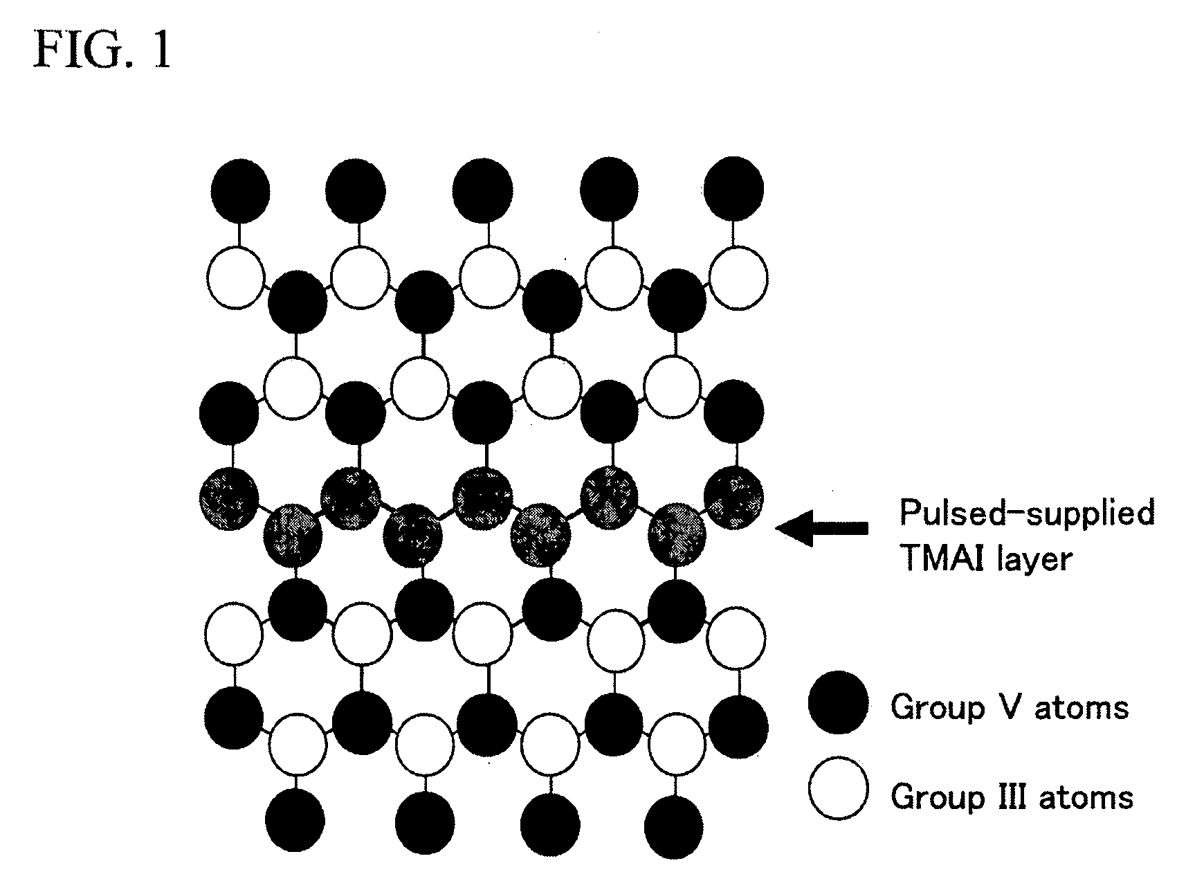
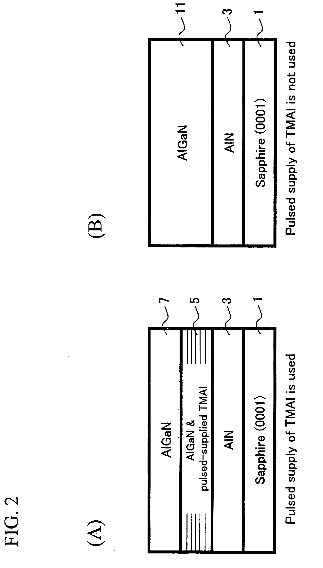
[0033]Prior to description of an embodiment of the present invention, there will be described considerations of the deep ultraviolet light emitting device by the inventor. The inventor has come to realize that controlling the polarity of group III compounds, such as AlGaN-based compounds, is very important. For example, when AlN is to be grown on a sapphire substrate, the polarity of AlN is unstable, and it is important to control the polarity of AlN to be the stable group III polarity. The inventor has found that the stable group III polarity can be achieved by pulsed supply of TMAl.

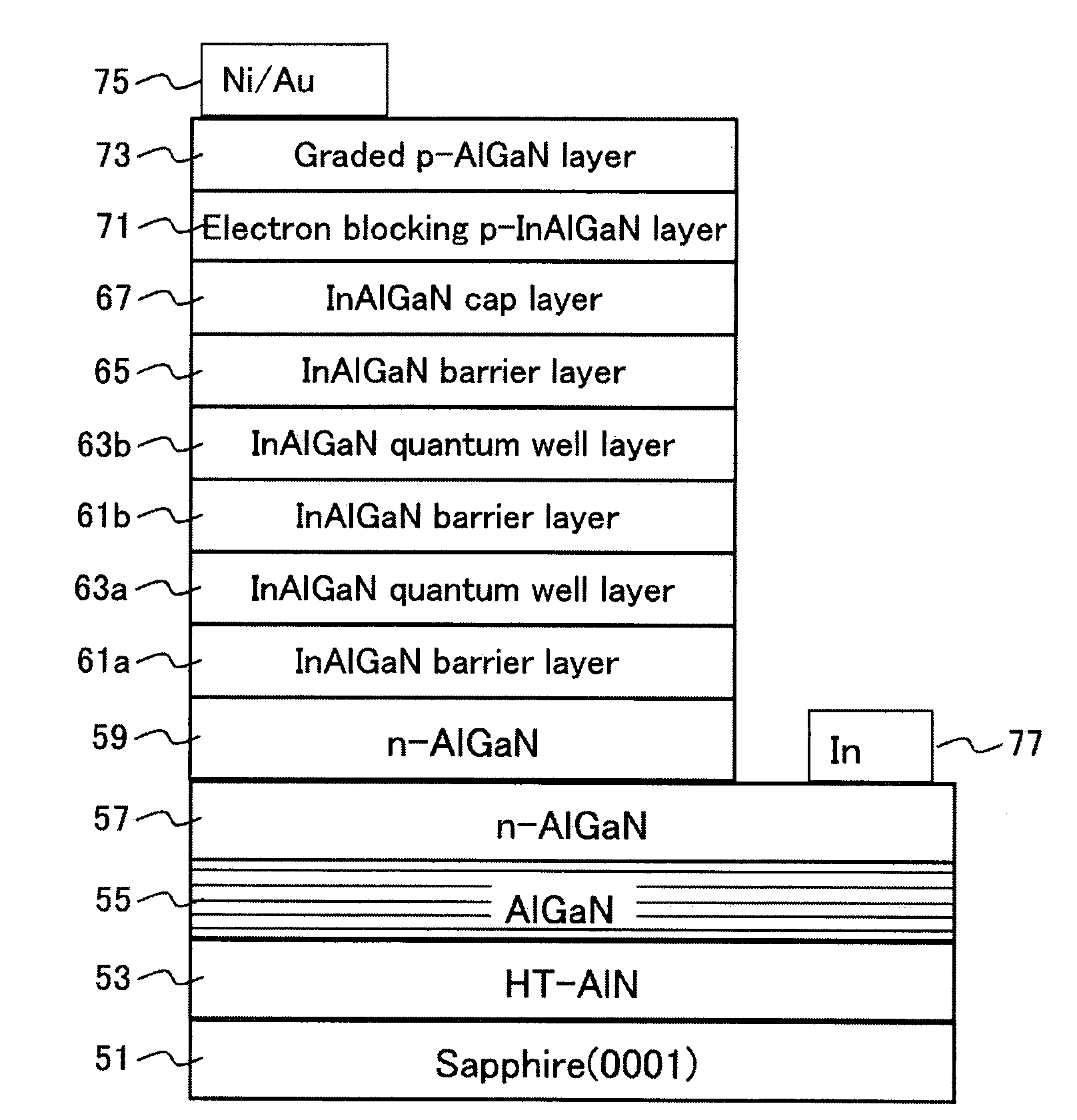
[0034]In the following, an optical semiconductor device and a manufacturing method therefor according to an embodiment of the present invention will be described with reference to the drawings. FIG. 1 is a cross-sectional view showing an atomic structure composed of group III atoms and group V atoms formed on a sapphire substrate. As shown in FIG. 1, a pulsed-supplied TMAl layer is built into a sample h...


PUM


Abstract

To provide an elemental technique for improving the emission intensity of deep ultraviolet light from a light emitting layer made of an AlGaInN-based material, in particular, an AlGaN-based material. First, an AlN layer is grown on a sapphire surface. The AlN layer is grown under a NH3-rich condition. The TMAl pulsed supply sequence includes growing an AlGaN layer for 10 seconds, interrupting the growth for 5 seconds to remove NH3, and then introducing TMAl at a flow rate of 1 sccm for 5 seconds. After that, the growth is interrupted again for 5 seconds. Defining this sequence as one growth cycle, five growth cycles are carried out. By such growth, an AlGaN layer having a polarity of richness in Al can be obtained. The above sequence is described only for illustrative purposes, and various variations are possible. In general, the Al polarity can be achieved by a process of repeating both growth interruption and supply of an Al source.

Description

BACKGROUND OF THE INVENTION[0001]1. Field of the Invention[0002]The present invention relates to an optical semiconductor device and a manufacturing method therefor. In particular, it relates to a technology of a deep ultraviolet light emitting device using a group III-V compound semiconductor.[0003]2. Background Art[0004]In recent years, in technical fields of semiconductor light emitting devices using PN junction, such as light emitting diodes and laser diodes, nitride semiconductors containing nitrogen as a group-V element have been drawing lots of attention, and research and development thereof have been actively carried out. Nitride semiconductors, such as AlN, GaN and InN, are direct transition semiconductors. Furthermore, a ternary or quaternary mixed crystal is capable of emitting light from infrared rays to deep ultraviolet rays by changing the band gap by appropriately determining the composition.[0005]Furthermore, a semiconductor light emitting device that has a light emi...

Claims


Application Information

Patent Timeline
IPC IPC(8): H01L33/00H01L21/00H01L33/06H01L33/12H01L33/20H01L33/32
CPCH01L21/0242H01L21/02458H01L21/02502H01L21/02507H01L33/32H01L21/02546H01L21/0262H01L33/16H01L21/0254
Inventor HIRAYAMA, HIDEKIOHASHI, TOMOAKIKAMATA, NORIHIKO
Owner RIKEN
Why Eureka
Try Eureka