Manufacturing of low defect density free-standing gallium nitride substrates and devices fabricated thereof

a gallium nitride substrate and low defect density technology, which is applied in the direction of crystal growth process, polycrystalline material growth, chemically reactive gas growth, etc., can solve the problems of gan not being melted, unable to grow low-defect density iii-n layers, and unable to meet the requirements of gan melted, etc., to reduce the defect density of the nitride crystal layer 103

Active Publication Date: 2015-04-21
IV WORKS
View PDF18 Cites 6 Cited by
  • Summary
  • Abstract
  • Description
  • Claims
  • Application Information

AI Technical Summary

Benefits of technology

[0050]Thus, and as will become clearer in the following, the formation of pillars on a sacrificial bed allows reducing the Threading Dislocations in the nitride crystal layer.
[0060]As mentioned above, the pillars are made of a material compatible with GaN epitaxial growth. This allows reducing the defects in the nitride crystal layer 103. In one embodiment, the pillars are made of GaN.
[0074]In all cases, the method can comprise a step of deposition of a second sacrificial layer on the bottom of the pillars. This facilitates the removal of the nitride crystal layer 103 from the pillars 102.

Problems solved by technology

Unfortunately, the development of nitride materials has been hampered by problems in the processing technology of such materials.
One problem in the development of Group III-N devices is the lack of gallium nitride bulk substrates of acceptable usable area or of lattice-matched substrates for growth of low-defect density III-N layers.
GaN cannot be melted and pulled from a boule like silicon, gallium arsenide, or sapphire, because at usual pressures its theoretical melting temperature exceeds its dissociation temperature.
Substantial difficulties have been shown when attempting to obtain large-area crystals of any Group III-nitride that could provide suitable substrates for device fabrication.
This technology has been developed at UNIPRESS (Poland), but the size of the substrate (˜1 cm2) and the volume of the potential mass production do not reach by far the industrial needs.
The techniques currently used for the fabrication of relatively high quality GaN and related layers involve the heteroepitaxial deposition of a GaN device layer onto a suitable but non-ideal substrate.
All heteroepitaxial substrates present challenges to the high-quality deposition of GaN, in the form of lattice and thermal mismatch.
Thermal mismatch is caused by differences in the thermal expansion coefficient between dissimilar materials.
However, even this method cannot compensate the lattice-mismatch between the substrate and the crystal, and the GaN film has still numerous defects.
Such large mismatches lead to the formation of very high densities of threading dislocations (˜109 cm−2) and eventually cracks.
Above a film thickness of approximately 10 microns, the stress levels exceed the fracture limits of the GaN, and cracking and peeling of the film may result.
The occurence of extended defects (threading dislocations, stacking faults, and antiphase boundaries) leads to significantly deteriorated performances and results in a shortened operating lifetime of devices.
More specifically, the dislocations behave as nonradiative centres, thus reducing the light-emitting efficiency of light-emitting diodes and laser diodes made from these materials.
Although threading dislocations have not prevented the development of high-brightness light-emitting diodes, they limit the lifetime and cause catastrophic failure in laser diodes.
They also cause excessive reverse-bias leakage currents in p-n junction devices such as high electron-mobility transistors, field-effect transistors and other electronic devices.
Further, the dislocations can act as strong scattering centres for carriers, thus reducing the mobility of electrons and holes unfavourably, limiting the performance of many semiconductor devices.
Even though ELO or pendeo technologies have significantly improved the quality of heteroepitaxial GaN, some drawbacks remain and are difficult to overcome.
Whatever the ELO process, coalescence boundaries are created that are regions of poor quality.
Therefore, optoelectronic devices should be fabricated on the good part of the ELO surface, thereby requiring complex technology.
Besides, getting thick ELO layers won't result in a disappearance of the coalescence boundaries, but conversely more likely in a spreading of this defective region.
Because HVPE was unable to produce p-type GaN, it was largely abandoned in the early 1980s.
As the layer becomes thicker, this leaves primarily edge dislocations with larger separation, therefore interactions become less and less likely and a further decrease of the density of TDs becomes difficult.
Actually, these TDs reduction mechanisms are very inefficient, and a closer look at the reduction mechanisms show that the most efficient reduction process comes from mixed dislocations.
ELO technologies have also been implemented in HVPE, but due to the high growth rate, wide pitch of the ELO openings in masks are required and new dislocations are often generated.
This however has proven to be a difficult task.
In GaN, the mechanisms are not yet fully established; however the implantation of hydrogen is used to create a brittle region in an ELO quality GaN / sapphire.

Method used


Image

  • Manufacturing of low defect density free-standing gallium nitride substrates and devices fabricated thereof
  • Manufacturing of low defect density free-standing gallium nitride substrates and devices fabricated thereof
  • Manufacturing of low defect density free-standing gallium nitride substrates and devices fabricated thereof

Examples


example 1

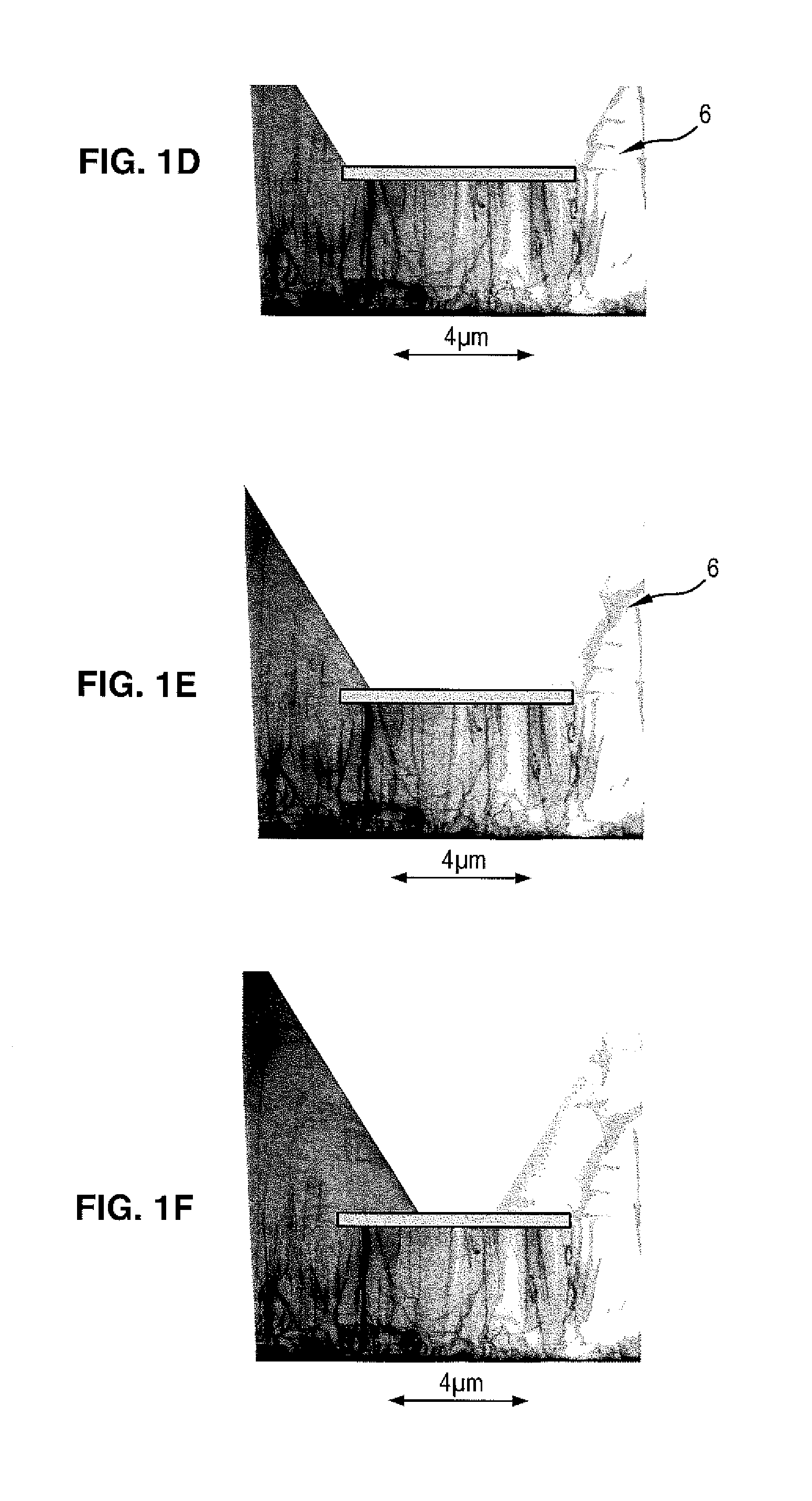
The Method of Manufacturing Such Substrates Comprises Several Steps as Schematically Shown on FIGS. 1 and 2

[0152]Epitaxial growth is carried out using preferably by Metal Organic Vapour Phase Epitaxy (MOVPE) for the fabrication of GaN pillars, even though other vapour phase epitaxy techniques such as Halide Vapour Phase Epitaxy (HVPE) and close space Vapour Phase transport (CSVT, also refereed as sublimation) can also be used.

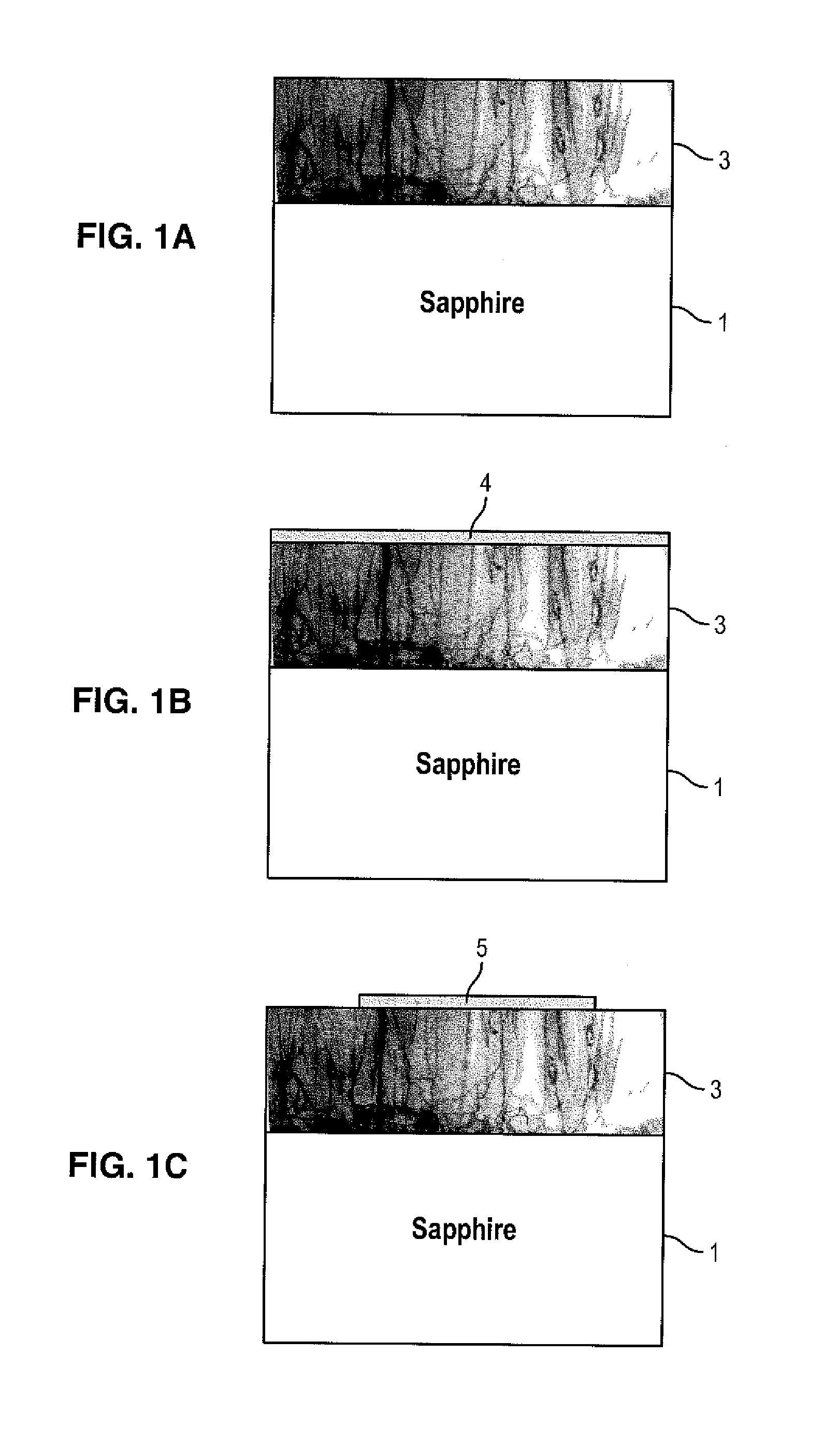
[0153]The substrate 1 generally has a thickness of a few hundred μm (in particular approximately 300 μm) and may be chosen from the group consisting of sapphire, ZnO, 6H—SiC, 4H—SiC, 3C—SiC, Si, LiGaO2, LiAIO2, MgAI2O4, ZrB2, GaAs, HfB2, AIN, GaN, and advantageously is sapphire (0001).

[0154]The following paragraphs are directed to a preferred process to produce the GaN layer 3.

[0155]This process for producing a layer of gallium nitride (GaN) is remarkable in that it comprises the deposition on a substrate of a silicon nitride layer functioning as a nanomask and...

example 2

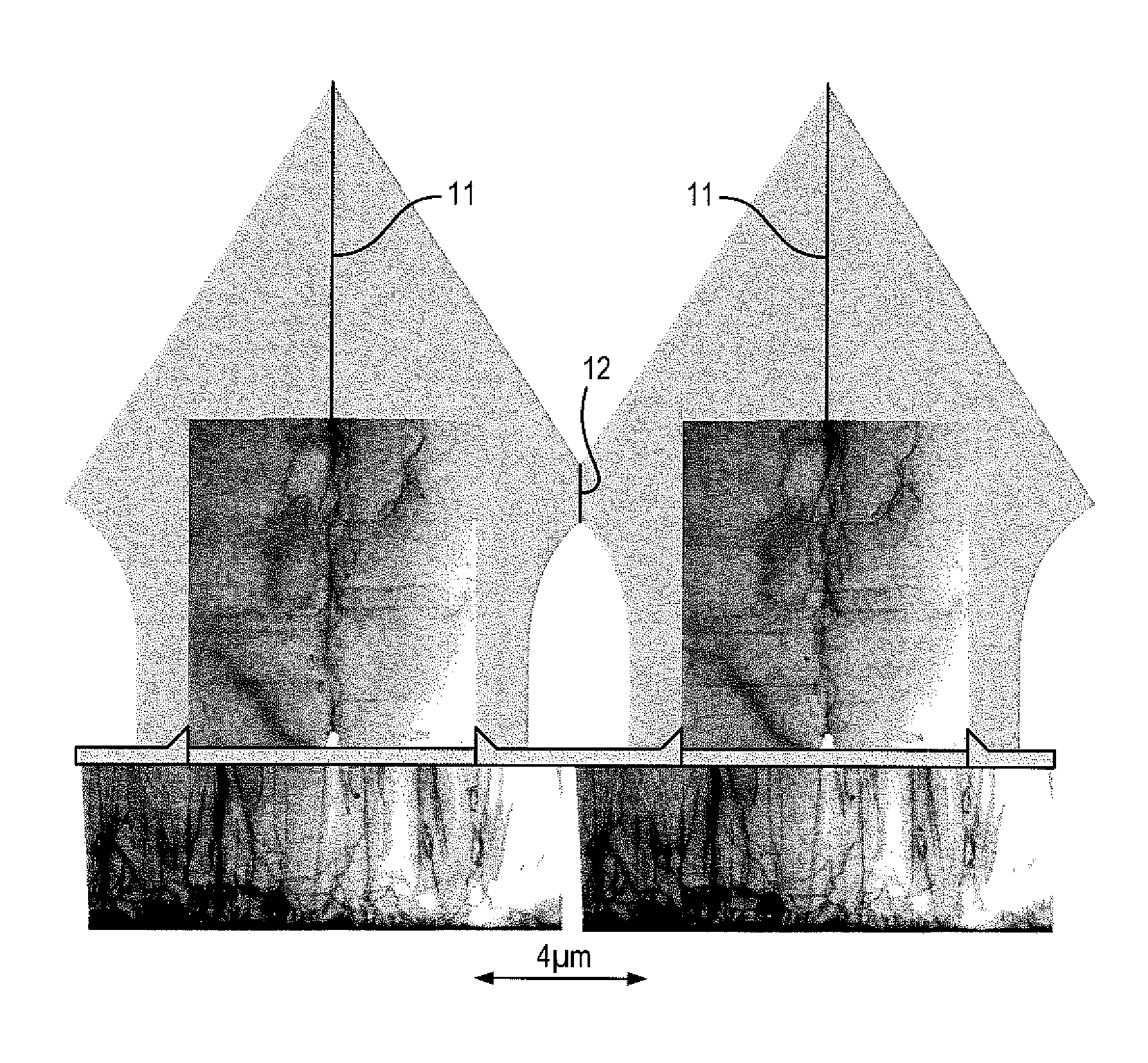
[0208]In example 2 however, after grooving the stripes to form pillars, the top mask 8 is not removed. Growth is allowed to restart in MOVPE.

[0209]As expected, growth starts from the {11-20} facets resulting from the RIE groove to finally coalescence into triangular stripes with {11-22} lateral facets as in example 1. The FIG. 8 schematically shows the evolution of the facets structure as growth proceeds.

[0210]At this stage, the structure is introduced in the multiwafer HVPE reactor and growth takes place according one of the variations described in example 1. After all the technological processes described in example 1, a free standing GaN wafer presenting TDs densities6 cm−2, that are uniformly distributed on the top Ga face surface is obtained. Indeed, once again, the HVPE step inducing multiple TD bendings results in a redistribution of TD at the coalescence boundaries from the MOVPE steps.

example 3

[0211]In example 3 the mask pattern for both the ELO process and the groove of pillars is a two dimensional array of hexagons (see FIG. 9A). The ELO GaN is grown as in example 1. When the first step of MOVPE ELO is achieved, a second mask consisting in an array of hexagons as shown in FIG. 9A is deposited exactly above the first one. Afterward RIE etching, a “honeycomb” structure is formed (see FIG. 8B). Conversely to previous examples, at this stage, etching can be achieved, at least partially, from the top surface. This will make the final separation easier.

[0212]These MOVPE / sapphire templates are introduced in a multiwafer HVPE reactor operating at low pressure, and the rest of the process follows previous examples. After all the technological processes described in example 1, a free standing GaN wafer presenting TDs densities6 cm−2, that are uniformly distributed on the top Ga face surface is obtained.


PUM

PropertyMeasurementUnit
thicknessaaaaaaaaaa
operating life-timeaaaaaaaaaa
thickaaaaaaaaaa

Abstract

The invention relates to a method for manufacturing a single crystal of nitride by epitaxial growth on a support (100) comprising a growth face (105), the method comprising the steps of formation of a sacrificial bed (101) on the support (100), formation of pillars (102) on said sacrificial bed, said pillars being made of a material compatible with GaN epitaxial growth, growth of a nitride crystal layer (103) on the pillars, under growing conditions such that the nitride crystal layer does not extend down to the support in holes (107) formed between the pillars, and removing the nitride crystal layer from the support.

Description

FIELD OF THE INVENTION[0001]The present invention concerns high quality free standing gallium nitride wafers suitable for the subsequent growth of efficient device structures and a method of manufacture thereof.[0002]More specifically, the invention relates to a process for growth of low dislocation density GaN on a substrate, to a process for epitaxial growth where the lateral and vertical growth rates of the material are controlled by growth conditions, to a process of separation from the starting substrate.[0003]The present invention also relates to a nitride semiconductor wafer having a GaN crystal formed by such a method and a nitride semiconductor device produced therefrom.DESCRIPTION OF THE STATE OF THE ART[0004]GaN-based compound semiconductors, such as gallium nitride (GaN), the ternary alloys, indium gallium nitride (InGaN) and gallium aluminium nitride (GaAIN) and even the quaternary (AlGaInN) are direct band gap semiconductors. Their gaps cover wavelengths extending from...

Claims


Application Information

Patent Timeline
Patent Type & Authority Patents(United States)
IPC IPC(8): H01L21/20C30B25/18C30B29/40H01L21/02
CPCC30B25/18C30B29/406H01L21/0237H01L21/0242H01L21/02458H01L21/0254H01L21/0262H01L21/02639H01L21/0265H01L21/02647C30B25/02C30B29/38
Inventor BEAUMONT, BERNARDFAURIE, JEAN-PIERRE
Owner IV WORKS
Why Eureka
Try Eureka