

Co-packaged high-side and low-side nmosfets for efficient dc-dc power conversion
a technology of dc-dc power conversion and high-side and low-side nmosfets, which is applied in the direction of semiconductor devices, semiconductor/solid-state device details, electrical apparatus, etc., can solve the problems of reducing the chip area of high-side and/or low-side chips, the size of power devices, and the cost and number of dc packages, so as to reduce the parasitic inductances associated, the effect of less space and less cos
- Summary
- Abstract
- Description
- Claims
- Application Information
AI Technical Summary
Benefits of technology
Problems solved by technology
Method used
Image

Examples
Embodiment Construction
[0024]Although the following detailed description contains many specific details for the purposes of illustration, anyone of ordinary skill in the art will appreciate that many variations and alterations to the following details are within the scope of the invention. Accordingly, the examples of embodiments of the invention described below are set forth without any loss of generality to, and without imposing limitations upon, the claimed invention.
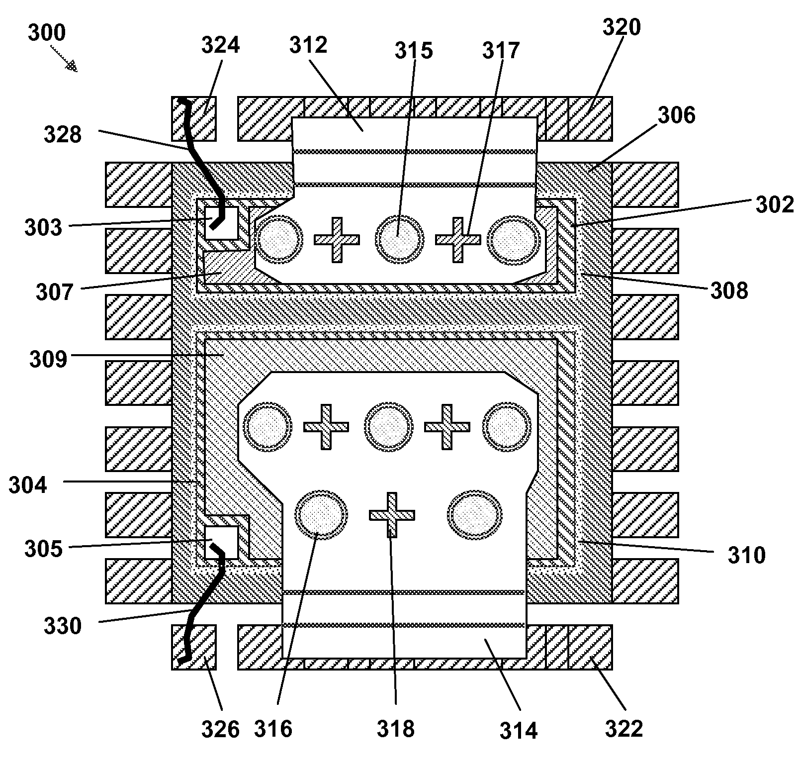
[0025]As discussed above, power converters that use NMOSFET power devices typically have three components: a gate driver IC, a high-side NMOSFET and a low-side NMOSFET. Conventionally, the high-side and low-side NMOSFETs are built on two separate die pads within one package. One possible approach to reducing the number of components is to use a combination of PMOSFET and NMOSFET power devices. If, e.g., the high-side power device is a PMOSFET device and the low-side power device is an NMOSFET device, both power devices may be attached to t...
PUM
 Abstract
Description
Claims
Application Information