Electron-emitting device and manufacturing method thereof

a technology of electron emission and manufacturing method, which is applied in the manufacture of electrode systems, electric discharge tubes/lamps, spark plugs, etc., can solve the problems of difficult elongation of the length of the gap, shortened space efficiency, and stenosis portion gap formation, etc., to achieve small characteristic variation, low power consumption, and sufficient electron emission amount

Inactive Publication Date: 2009-03-05
CANON KK
View PDF17 Cites 9 Cited by
  • Summary
  • Abstract
  • Description
  • Claims
  • Application Information

AI Technical Summary

Benefits of technology

[0008]An object of the present invention is to provide an electron-emitting device, which can obtain a sufficient electron emission amount by elongating the length of the gap. In addition, the object of the present invention is to control the position of the gap in the conductive film and provide an art for manufacturing an electron-emitting device having a small characteristic variation by low power consumption.

Problems solved by technology

However, according to any of the methods disclosed in JP-B No. 2627620 and JP-B No. 3647436, forming a stenosis portion in the conductive film, then, a gap is formed in the stenosis portion.
In such a method, it is hard to elongate the length of the gap because space efficiency is lowered (namely, a space needed for mounting the conductive film is made large).

Method used


Image

  • Electron-emitting device and manufacturing method thereof
  • Electron-emitting device and manufacturing method thereof
  • Electron-emitting device and manufacturing method thereof

Examples


example 1

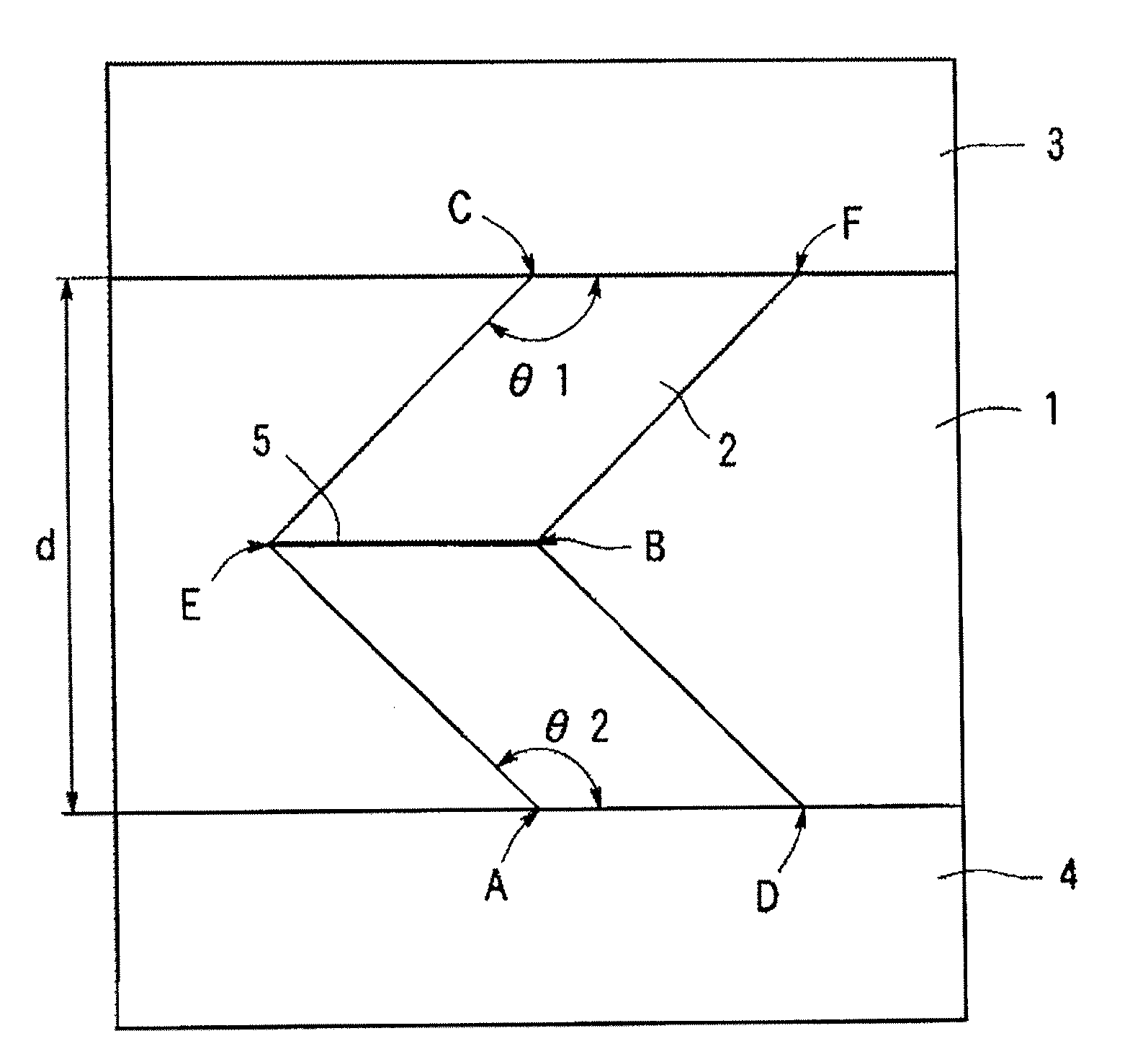
[0095]The surface conduction electron-emitting device having the conductive film 2 formed in a shape shown in FIG. 1 was manufactured. The manufacturing steps are as follows.

[0096]Step a: A quartz substrate (SiO2 substrate) as the substrate 1 was sufficiently cleaned by an organic solvent. Then, the electrodes 3 and 4 made of Pt were formed on the substrate 1. An electrode gap d, a film thickness, the length of opposite sides of the electrodes 3 and 4 were defined to be 10 μm, 0.04 μm, and 200 μm, respectively (opposite sides of the electrodes 3 and 4 were defined to be parallel with each other).

[0097]Step b: A droplet of a solution having an organic metallic compound was dropped between the electrodes 3 and 4 of the substrate 1 by using an ink jet method. Then, by drying the dropped solution, an organic metallic thin film was formed. After that, by burning the organic metallic thin film by a clean oven, the conductive film 2 made of palladium oxide (PdO) particles was formed.

[0098]...

example 2

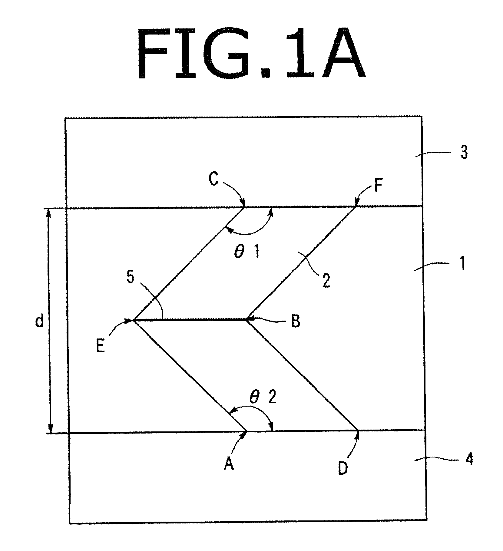
[0103]In the conductive film 2 according to the example 1, both of θ1 and θ2 were defined to be 150°, and others were the same as the example 1.

example 3

[0104]In the conductive film 2 according to the example 1, θ2 was defined to be 135°, and θ1 was defined to be 150° (a shape as shown in FIG. 19). Others were the same as the example 1.


PUM


Abstract

A manufacturing method of an electron-emitting device according to the present invention includes the steps of: preparing a substrate having a first electrode and a second electrode, and a conductive film for connecting the first electrode and the second electrode; and forming a gap on the conductive film by applying a voltage between the first electrode and the second electrode; wherein a planar shape of the conductive film has a V-shape portion between the first electrode and the second electrode.

Description

BACKGROUND OF THE INVENTION[0001]1. Field of the Invention[0002]The present invention relates to an electron-emitting device that is used for a flat panel display, and a manufacturing method of the electron-emitting device.[0003]2. Description of the Related Art[0004]A surface conduction electron-emitting device utilizes a phenomenon such that electron-emission is generated by applying a current on a film surface of a conductive film of a small area that is formed on a substrate in parallel. It has been popular that an electron emission portion is formed on the conductive film of the surface conduction electron-emitting device in advance by a conducting process (a forming). Specifically, the electron emission portion is formed by applying a direct voltage or a very slow boost voltage (for example, about 1 V / minute) to the opposite ends of the conductive film. Thereby, the conductive film is locally damaged, transformed, or modified, and then, as an electron emission portion, an elec...

Claims


Application Information

Patent Timeline
Patent Type & Authority Applications(United States)
IPC IPC(8): H01J1/00H01J9/00
CPCH01J1/316H01J2201/3165H01J9/027
Inventor TAKADA, HIROKOAZUMA, HISANOBUIBA, JUN
Owner CANON KK
Why Eureka
Try Eureka