Linearizer

a linearizer and line-type technology, applied in the field of line-type devices, can solve the problems of difficult control of the boundary of an active region, limited reliability of the current anode metal, and increased cost, so as to reduce the insertion loss, and reduce the characteristic variation

Active Publication Date: 2015-11-26
MITSUBISHI ELECTRIC CORP
View PDF2 Cites 8 Cited by
  • Summary
  • Abstract
  • Description
  • Claims
  • Application Information

AI Technical Summary

Benefits of technology

[0011]Because there are two output side circuits in the present invention, an impedance of the branch circuit in the present embodiment is lower than that in the example having one output side circuit. Thus, high-frequency signals are less likely to be affected by the diode, and it is thereby possible to reduce insertion loss of the diode. Therefore, even using the diode having a large unit anode width whose insertion loss is likely to increase, it is possible to reduce insertion loss. The diode having a large unit anode width has a smaller characteristic variation and thereby has a high manufacturing yield. Thus, the present invention can increase the yield while reducing insertion loss.
[0012]When amplifiers are configured in a tournament form, there tends to be extra space in layout near a branch point. In the present invention, since the linearizer is provided at this branch point, it is possible to insert the linearizer while preventing the circuit area from increasing. This prevents the area occupied by an expensive epitaxial substrate from increasing, and can thereby reduce cost.

Problems solved by technology

Therefore, the area occupied by an expensive epitaxial substrate increases, resulting in a problem of cost increase.
Second, when an overcurrent is passed through an anode metal, electromigration occurs in an anode electrode, and therefore the current capacity of the anode metal is limited in terms of reliability.
On the other hand, it is difficult to control the boundary of an active region that determines the unit anode width Wau in a wafer process and a variation of the unit anode width Wau increases.
Therefore, the problem is that there is a trade-off relationship between the insertion loss and manufacturing yield.

Method used


Image

  • Linearizer
  • Linearizer
  • Linearizer

Examples


first embodiment

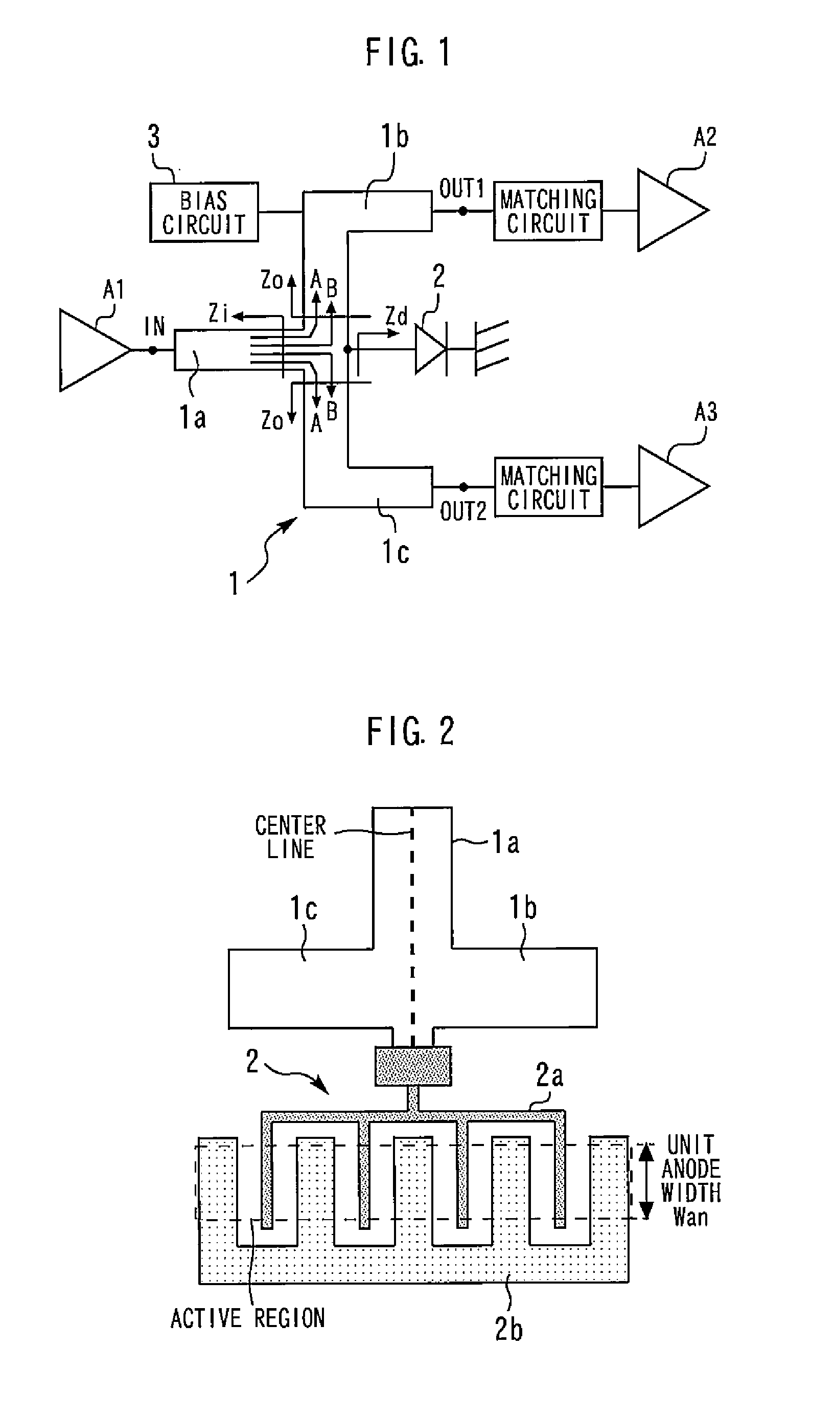
[0027]FIG. 1 is a diagram illustrating a linearizer according to a first embodiment of the present invention. FIG. 2 is a partially enlarged view of the linearizer in FIG. 1. The linearizer is inserted between an upstream amplifier A1 and downstream amplifiers A2 and A3. A branch circuit 1 of the linearizer has an input transmission line 1a and output transmission lines 1b and 1c. The input transmission line 1a is connected between an input terminal IN and a branch point. The output transmission line 1b is connected between a branch point and an output terminal OUT1, and the output transmission line 1c is connected between the branch point and an output terminal OUT2.

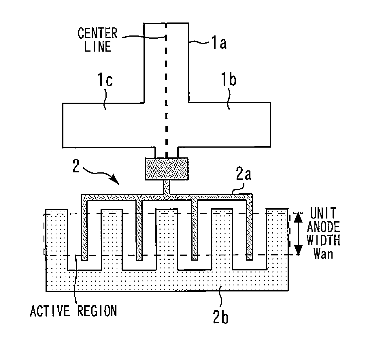
[0028]An anode of a diode 2 is connected to the branch point of the branch circuit 1 and a cathode thereof is grounded. In the present embodiment, the anode of the diode 2 is connected on an extension of a center line of the input transmission line 1a. A bias circuit 3 biases the diode 2 in a forward direction. Anode fi...

second embodiment

[0035]FIG. 6 is a diagram illustrating a linearizer according to a second embodiment of the present invention. The cathode of the diode 2 is grounded via a via hole 4. In a high-frequency band, an inductance of the via hole 4 cannot be ignored. Thus, in the present embodiment, an inductor 5 is connected between the cathode of the diode 2 and the ground. A design is performed assuming that the inductance of the via hole 4 is LVH and the inductance of the inductor 5 is Lc so as to satisfy equation (4).

Zd+ω(Lc+LVH)>ZiZo2Zi+Zo(4)

[0036]FIG. 7 is a diagram illustrating an AMAM characteristic of the linearizer according to the second embodiment of the present invention. An inductance component from the cathode of the diode to an ideal ground is used as a parameter. In the case of a substrate having a thickness of 100 μm, the inductance LVH of the via hole 4 is on the order of 30 pH. When the cathode of the diode 2 is directly connected to the via hole 4, although passage loss is approximat...

third embodiment

[0037]FIG. 8 is a diagram illustrating a linearizer according to a third embodiment of the present invention. A resistor 6 is connected between the cathode of the diode 2 and ground. A desired characteristic can be obtained by designing an appropriate matching circuit including the resistance value of this resistor 6. The rest of the configuration and effects are similar to those of the first embodiment.


PUM


Abstract

A linearizer includes: a branch circuit having an input transmission line connected between an input terminal and a branch point, a first output transmission line connected between the branch point and a first output terminal, and a second output transmission line connected between the branch point and a second output terminal; a diode having an anode connected to the branch point and a cathode; and a bias circuit biasing the diode.

Description

BACKGROUND OF THE INVENTION[0001]1. Field of the Invention[0002]The present invention relates to a linearizer connected to a high-frequency amplifier to improve distortion characteristics.[0003]2. Background Art[0004]In recent years, research and development into transistors using a nitride semiconductor (e.g., GaN) are being actively carried out, and an application example thereof is a high output amplifier for communication. Amplifiers using GaN are enabled to have higher output than conventional compound semiconductors (e.g., GaAs). However, particularly an AMAM characteristic (output level characteristic when an input level is increased) deteriorates due to GaN-specific soft compression in which a gain slowly decreases from low input power.[0005]Thus, as analog predistortion that compensates for the AMAM characteristic, linearizers using a diode are used (e.g., see Japanese Patent Application Laid-Open No. 2012-244545). Linearizers having a small circuit configuration are partic...

Claims


Application Information

Patent Timeline
Patent Type & Authority Applications(United States)
IPC IPC(8): H03F1/32
CPCH03F1/3258H03F2201/3215H03F2200/387H03F1/32H03F3/195H03F3/211H03F3/245H03F3/68H03F3/602
Inventor KANAYA, KO
Owner MITSUBISHI ELECTRIC CORP
Why Eureka
Try Eureka