Plasma display panel drive circuit and plasma display apparatus

a drive circuit and display panel technology, applied in the direction of instruments, static indicating devices, etc., can solve the problems of increasing the number of elements that compose the pdp drive circuit and increasing the installation area of the circuit, and the inability to generate normal drive waveforms, so as to reduce the impedance, improve the recovery ratio of electric power accumulated, and reduce power consumption

Inactive Publication Date: 2009-03-05
PANASONIC CORP
View PDF10 Cites 20 Cited by
  • Summary
  • Abstract
  • Description
  • Claims
  • Application Information

AI Technical Summary

Benefits of technology

[0137]As described above, according to the present embodiment, a configuration with diodes D11 and D12 provided to the voltage clamp circuit of the sustain pulse generation circuit 5101 can electrically separate the constant-voltage power supply V1 and GND of the voltage clamp circuit from the main discharge path without disposing a switching element between the sustain pulse generation circuit 5101 and the reset waveform generation circuit 52. Consequently, it is possible to reduce impedance in the main discharge path X from the coil L1 of the power recovery circuit 80 to scan electrodes SC1 through SCn, to improve the recovery ratio of electric power accumulated in the capacitive load of PDP 10, and to achieve reduction of power consumption.
[0138]Furthermore, since a drive circuit can be configured by the use of diodes with large rated values, as compared to the case in which MOSFETs and other switching elements are used, the number of elements that compose the drive circuit can be reduced.
[0139]Furthermore, since a configuration with the switching element S11 which is connected to the diode D11 in parallel and can switch from shutting off or passing or vice versa the current that flows from the main discharge path X to the constant-voltage power supply V1 is adopted. Thus even if the diode D11 comes into an electrically disconnected state, by turning on the switching element S11, it is possible to allow the current to pass from the main discharge path X to the constant-voltage power supply V1 via the switching element S11 and the diode connected to the switching...

Problems solved by technology

However, in the configuration shown in FIG. 26, the point is not changed in that a large number of MOSFETs are used to configure switching elements S101 and S102 to proof large current of several hundreds of ampere which instantaneously flows when PDP 10 is driven, and consequently, the problem of increasing the number of elements which compose the PDP drive circuit ...

Method used


Image

  • Plasma display panel drive circuit and plasma display apparatus
  • Plasma display panel drive circuit and plasma display apparatus
  • Plasma display panel drive circuit and plasma display apparatus

Examples


embodiment 1

1-1 Configuration

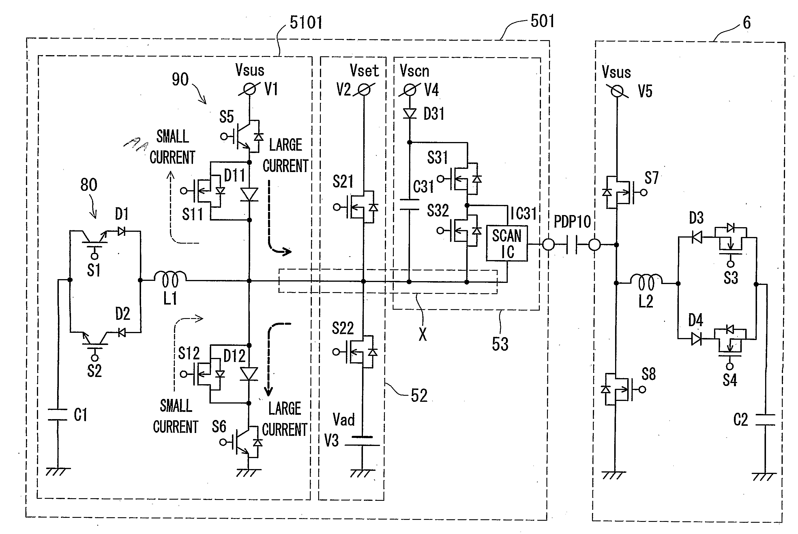
[0090]FIG. 1 is an illustration that shows a configuration of a PDP drive circuit in embodiment 1 of the present invention. The PDP drive circuit shown in FIG. 1 is a circuit which applies drive voltage to electrodes of a plasma display panel (PDP) to drive the PDP. Before explaining the configuration and operation of the PDP drive circuit in detail, description is made on the PDP configuration and operation.

1-1-1 PDP Structure

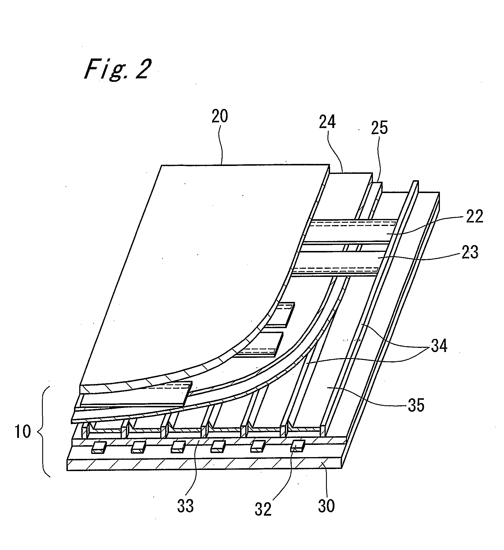
[0091]FIG. 2 is a perspective view that indicates PDP structure. On a front plane 20 made of glass, which is the first substrate, a plurality of display electrodes forming a pair with stripe-form scan electrode 22 and sustain electrode 23 are formed. A dielectric layer 24 is formed to cover the scan electrode 22 and sustain electrode 23, and a protective layer 25 is formed on the dielectric layer 24.

[0092]On a back plane 30 which is the second substrate, a plurality of stripe-form data electrodes 32 covered with dielectric layer 33 are formed ...

embodiment 2

2-1 Configuration of PDP Drive Circuit

[0166]FIG. 13 is an illustration that indicates a configuration of PDP drive circuit in embodiment 2 of the present invention. Structure and electrode arrangement of PDP which the PDP drive circuit in the present embodiment is subject to drive, each drive voltage waveform which the PDP drive circuit in the present embodiment applies to each electrode of PDP 10, and electrical configuration of a plasma display apparatus in which the PDP drive circuit and PDP 10 of the present embodiment are same as those of embodiment 1. Thus descriptions on the relevant configuration and operation will be omitted.

[0167]As shown in FIG. 13, the PDP drive circuit in embodiment 2 of the present invention is equipped with a scan electrode drive circuit 508 and the sustain electrode drive circuit 6 which have power recovery circuits. The scan electrode drive circuit 508 has a sustain pulse generation circuit 5108, reset waveform generation circuit 52, and scan pulse ...

modification examples

2-4 Modification Examples

2-4-1 Modification Example 1

[0197]FIG. 14 is an illustration that indicates another example of the configuration of PDP drive circuit in embodiment 2 of the present invention. The PDP drive circuit shown in FIG. 14 has a scan electrode drive circuit 509 and a sustain electrode drive circuit 6, and the scan electrode drive circuit 509 has a sustain pulse generation circuit 5109, a reset waveform generation circuit 52, and a scanning pulse generation circuit 53.

[0198]When there is no need to apply negative voltage at the time of generating the reset waveform and no constant-voltage power supply with negative potential is used for the reset waveform generation circuit 52, as shown in FIG. 14, a voltage clamp circuit 91b of the sustain pulse generation circuit 5109 may be configured without using the diode D120 and the switching element S120 of FIG. 13. Even in this configuration, the same effects as described above can be obtained.


PUM


Abstract

A drive circuit for driving a plasma display panel (PDP) includes a pulse voltage generation circuit (5101) that contains main switching elements disposed on the high voltage side and on the low voltage side, is operable to generate a pulse voltage by operating the main switching elements in accordance with an output voltage from a first power supply (V1) and apply the pulse voltage to a PDP scan electrode and sustain electrode, and a reset voltage generation circuit (52) operable to generate a reset voltage in accordance with an output voltage from a second power supply (V2) and apply it to the PDP. The pulse voltage generator C circuit contains a first diode (D11) that prevents the voltage outputted by the reset voltage generation circuit from being applied backward to the first power supply and a first switching element (S11) connected to the first diode in parallel.

Description

TECHNICAL FIELD[0001]The present invention relates to a plasma display panel drive circuit, as well as plasma display apparatus, used for wall-mounted TV sets and large-size monitors.BACKGROUND ART[0002]An AC surface discharge type plasma display panel (hereinafter called “PDP”) which is typical as the AC type is constituted by arranging a front plate containing a glass substrate formed by disposing a scan electrode and a sustain electrode which carry out surface discharge and a back plate containing a glass substrate formed by disposing data electrodes oppositely in parallel so that both electrodes set up a matrix and a discharge space is formed in a gap, and by sealing the perimeter portion with sealing materials such as glass frit, etc. Between both substrates of the front plate and the back plate, discharge cells divided by bulkheads are provided, and in a cell space between these bulkheads, a phosphor layer is formed. In PDP of such configuration, ultraviolet rays are generated...

Claims


Application Information

Patent Timeline
IPC IPC(8): G09G3/10G09G3/28
CPCG09G3/2927G09G2310/066G09G3/2965G09G3/296
Inventor ARAI, YASUHIRONAKATA, HIDEKINAGAKI, TOSHIKAZUIKEDA, SATOSHI
Owner PANASONIC CORP
Why Eureka
Try Eureka