Liquid crystal display device

a liquid crystal display and display device technology, applied in non-linear optics, instruments, optics, etc., can solve problems such as light leakage, achieve the effect of reducing the overlap between the video signal line and the pixel electrode, superior contrast, and reducing alignment disturbances such as the reverse tilt domain

Inactive Publication Date: 2009-03-05
HITACHI DISPLAYS
View PDF4 Cites 6 Cited by
  • Summary
  • Abstract
  • Description
  • Claims
  • Application Information

AI Technical Summary

Benefits of technology

[0022]According to a first aspect of the present invention, in a structure in which light leakage by alignment disturbance is prevented by the video signal line and the light-shielding film, a side in which a reverse tilt domain occurs is effectively light-shielded and the positional relationship between the video signal line and the light-shielding film is set considering the formation precision of the pattern and the positioning precision of the substrate, and, thus, a TN-type liquid crystal display device driven by the dot inversion driving method or the column inversion driving method which is bright and which has a superior contrast can be obtained.
[0023]According to another aspect of the present invention, because the pixel electrode and the video signal line are bent within a pixel, alignment disturbance such as the reverse tilt domain can be reduced, and the amount of overlap between the video signal line and the pixel electrode can be reduced. With such a structure, a TN-type liquid crystal display device driven by the dot inversion driving method or the column inversion driving method which is bright and which has a superior contrast can be obtained.
[0024]According to yet another aspect of the present invention, by tilting the pixel electrode and the video signal line in the same direction within a pixel and specifying the tilting angle, it is possible to reduce alignment disturbance such as the reverse tilt domain, and the amount of overlap between the video signal line and the pixel electrode for preventing the light leakage can be reduced. With such a structure, a TN-type liquid crystal display device driven by the dot inversion driving method or the column inversion driving method which is bright and which has a superior contrast can be obtained.

Problems solved by technology

Because the horizontal electric field disturbs the desired alignment of the liquid crystal molecules, that is, the horizontal electric field disturbs the alignment by the vertical electric field, a light leakage occurs during black display.

Method used


Image

  • Liquid crystal display device
  • Liquid crystal display device
  • Liquid crystal display device

Examples


first preferred embodiment

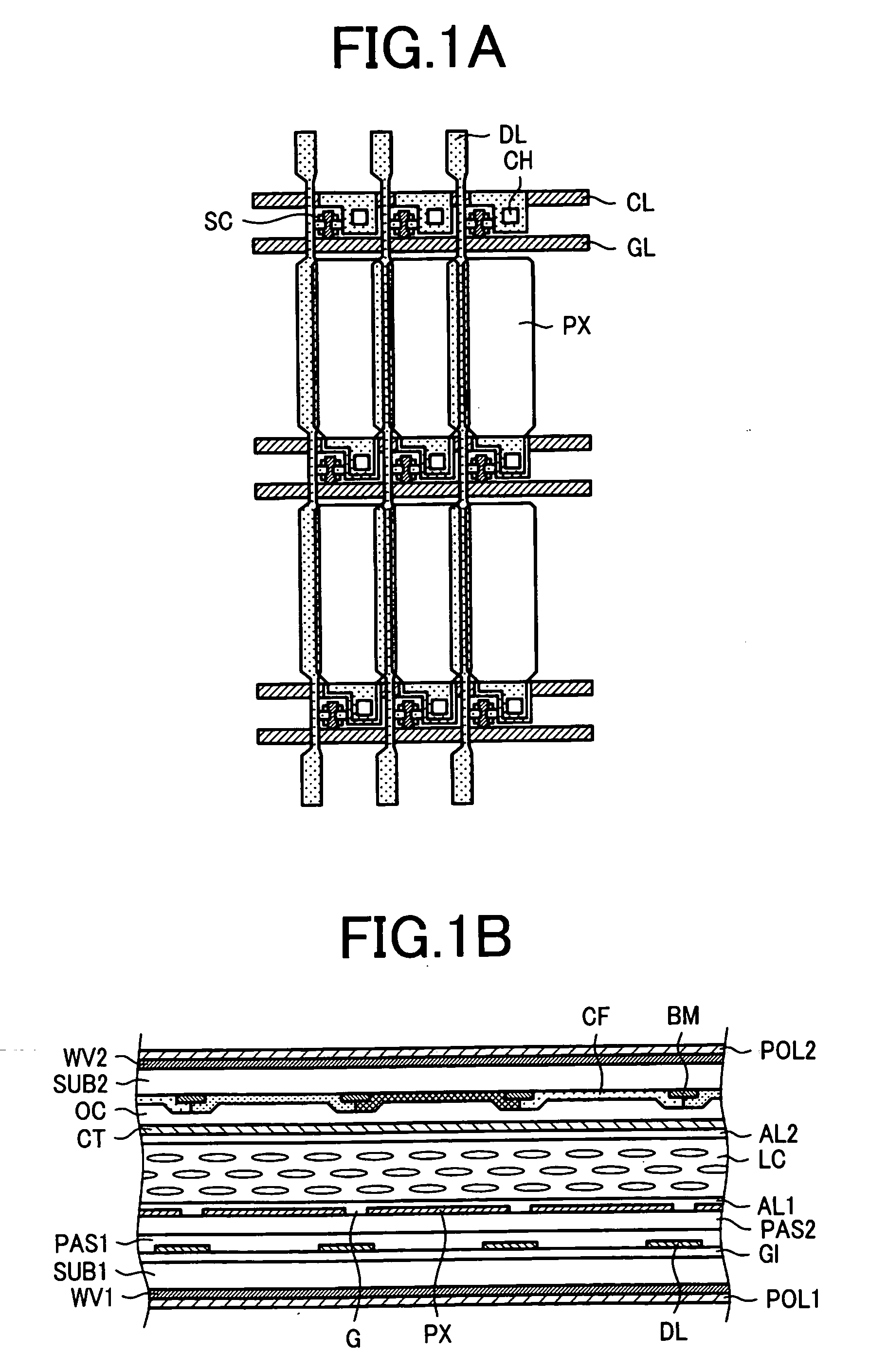
[0085]FIGS. 1A and 1B are schematic diagrams showing a principle of a first preferred embodiment of the present invention. FIG. 1 shows a liquid crystal display device with the three o'clock viewing angle. FIG. 1A is a plan view of the first substrate SUB1 and FIG. 1B is a cross sectional diagram of a state in which the firs substrate SUB1 and the second substrate SUB2 are combined. In the case of the three o'clock viewing angle, the disclination line due to the reverse tilt occurs at the left of the video signal line DL. Therefore, by increasing an amount of overlap between the pixel electrode PX and the video signal line DL at the left of the video signal line DL, it is possible to block only the portion corresponding to the disclination line and improve the contrast without causing a significant reduction in the aperture ratio. More specifically, the width of the video signal line DL is increased at the left of the video signal line DL.

[0086]In FIG. 1A, storage capacitor lines CL...

second preferred embodiment

[0098]In a second preferred embodiment of the present invention, the alignment disturbance is reduced by controlling the direction of the initial alignment vector of the first substrate SUB1 or of the second substrate SUB2 and the direction of the electric field between the pixels. FIGS. 4, 5A, and 5B are diagrams for explaining this structure. FIG. 4 shows a state in which the video signal line DL and an end of the pixel electrode PX overlap each other in the plan view. In FIG. 4, because the structure is in the ON state with dot inversion driving, a negative potential with respect to a potential on the opposing electrode CT (not shown) is applied to the pixel electrode PX at the left and a positive potential with respect to the potential on the opposing electrode CT is applied to the pixel electrode PX at the right. Therefore, an electric field EF is generated between the opposing pixel electrodes PX. In addition, because the initial alignment direction of the liquid molecules is ...

third preferred embodiment

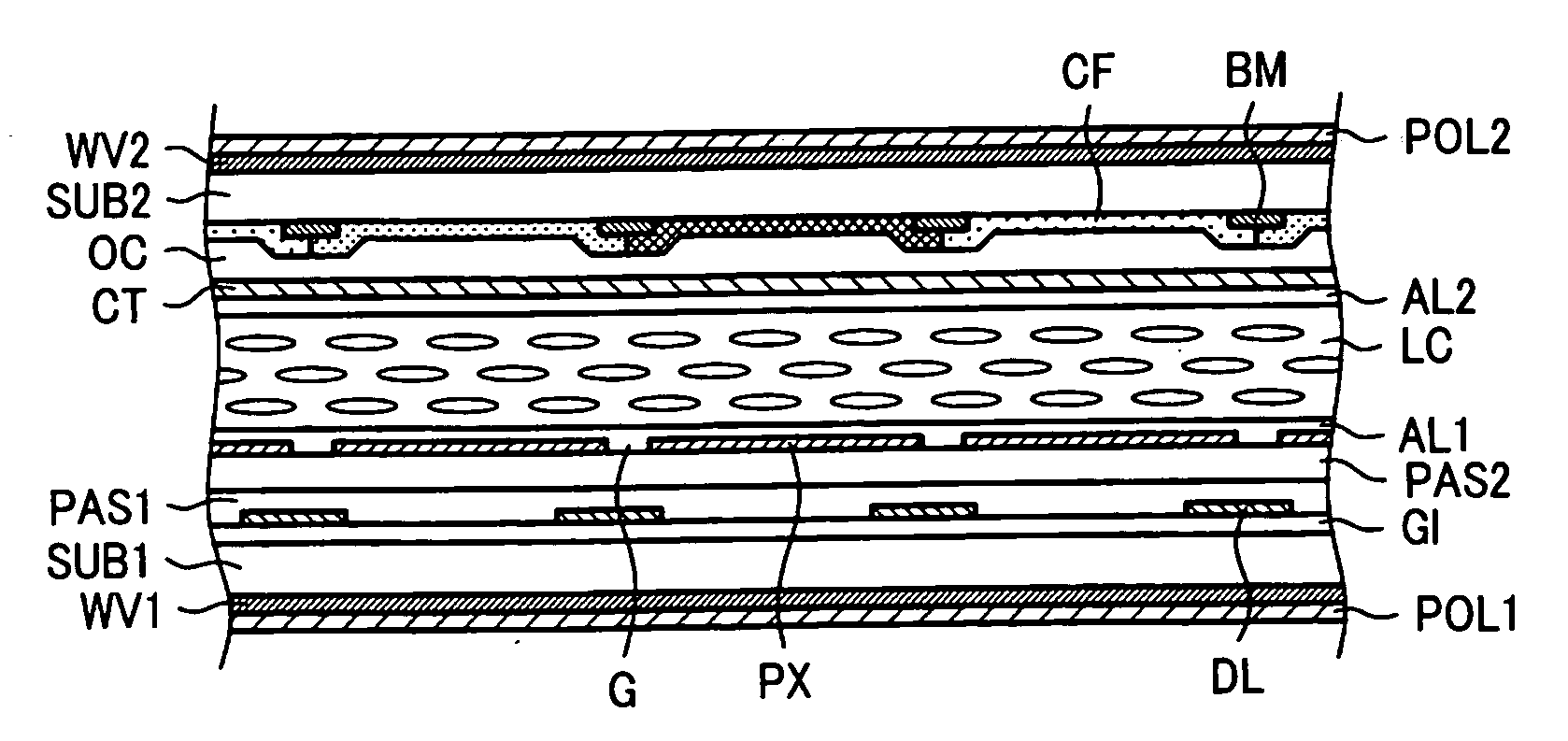
[0129]In the third preferred embodiment, the degree of alignment disturbance by the electric field between the pixel electrodes PX is reduced by controlling the thickness of the liquid crystal layer LC in the dot inversion driving with the three o'clock viewing angle. FIG. 11 is a cross sectional diagram in a direction parallel to the video signal line DL of the liquid crystal display device, that is, the y direction. In FIG. 11, the lower polarizer plate POL1 and the lower viewing angle expansion film WV1 are adhered under the first substrate SUB1. Scan lines GL and storage capacitor lines CL are formed at the inner side of the first substrate SUB1, and, over a gate insulating film GI which is formed over the scan line GL and the storage capacitor line CL, the thin film transistor (TFT) having the semiconductor layer SC, a drain electrode DE, and a source electrode SE is formed. The first passivation film PAS1 and the second passivation film PAS2 are formed covering the TFT, and th...


PUM

PropertyMeasurementUnit
angleaaaaaaaaaa
angleaaaaaaaaaa
angleaaaaaaaaaa

Abstract

Light leakage between pixel electrodes over a video signal line in a TN-type liquid crystal display device in which a dot inversion driving is applied with a three o'clock viewing angle is prevented. Pixel electrodes (PX) are formed on both sides of a video signal line (DL) of a first substrate (SUB1), and an end of the pixel electrode (PX) and the video signal line (DL) overlap each other. Over a second substrate (SUB2), a black matrix (BM) is formed in a portion corresponding to the video signal line (DL). By shifting the black matrix BM and the video signal line DL to the left with respect to a gap G between the pixel electrodes PX, it is possible to prevent light leakage caused by a disclination line (DS) which occurs by a horizontal electric field between pixel electrodes (PX).

Description

CROSS-REFERENCE TO RELATED APPLICATIONS[0001]The present application claims priority from Japanese application JP 2007-224106 filed on Aug. 30, 2007, the content of which is hereby incorporated by reference into this application.BACKGROUND OF THE INVENTION[0002]1. Field of the Invention[0003]The present invention relates to a liquid crystal display device, and, in particular, to a liquid crystal display device having a countermeasure to a light leakage in a dot-inversion driving method or in a column inversion driving method.[0004]2. Description of the Related Art[0005]In a liquid crystal display device, a first substrate on which pixel electrodes, thin film transistors (hereinafter referred to as “TFT”), etc. are formed in a matrix form and a second substrate on which color filters or the like are formed at positions corresponding to the pixel electrodes oppose each other, and liquid crystal is provided between the first substrate and the second substrate. A transmittance of light ...

Claims


Application Information

Patent Timeline
Patent Type & Authority Applications(United States)
IPC IPC(8): G02F1/1337
CPCG02F1/133512G02F1/1396G02F1/136286G02F1/133555
Inventor IGETA, KOICHINAGASHIMA, OSAMU
Owner HITACHI DISPLAYS
Why Eureka
Try Eureka