Techniques for Fabricating Nanowire Field-Effect Transistors

a field-effect transistor and nanowire technology, applied in the field of field-effect transistors, can solve the problems of difficult in-situ doping of nanowires during their growth, integrating nanowires into fet devices, and heavy in-situ doping

Active Publication Date: 2009-03-05
GLOBALFOUNDRIES US INC
View PDF2 Cites 93 Cited by
  • Summary
  • Abstract
  • Description
  • Claims
  • Application Information

AI Technical Summary

Benefits of technology

[0008]The present invention provides techniques for the fabrication of field-effect transistors (FETs) having nanowire channels. In one aspect of the invention, a method of fabricating a FET is provided. The method comprises the following steps. A substrate is provided having a silicon-on-insulator (SOI) layer. At least one nanowire is deposited over the SOI layer. A sacrificial gate is formed over the SOI layer so as to cover a portion of the nanowire that forms a channel region. An epitaxial semiconductor material is selectively grown from the SOI lay...

Problems solved by technology

Integrating nanowires in FET devices, however, presents several notable challenges.
First, trying to in-situ dope nanowires during their growth is difficult since dopants are incorporated into the nanowire from the gas-phase and/or by radial growth.
Third, heavy in-situ doping can lead to nanowire tapering, i.e., in germanium (Ge) nanowires, and loss of gold (Au) from the catalyst, i.e., in silicon (Si) nanowires doped with diborane.
Fourth, even if segmented doping along a nanowire body can be achieved, there are no simple methods to align the contacts and the gate to each se...

Method used


Image

  • Techniques for Fabricating Nanowire Field-Effect Transistors
  • Techniques for Fabricating Nanowire Field-Effect Transistors
  • Techniques for Fabricating Nanowire Field-Effect Transistors

Examples


Embodiment Construction

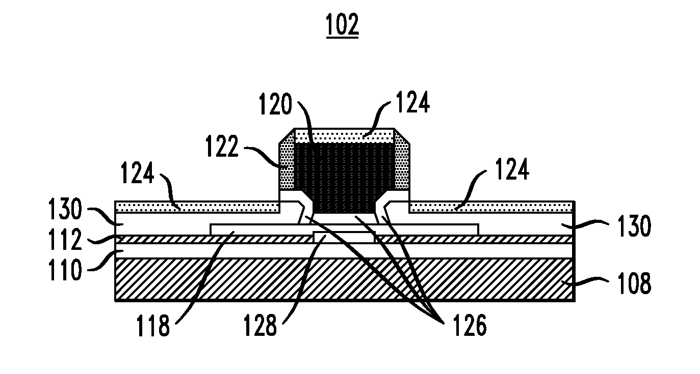
[0030]FIG. 1 is a diagram illustrating exemplary field-effect transistor (FET) 102 having a nanowire channel. For ease of depiction, the structures shown illustrated in FIG. 1 are not drawn to scale. Further, the cross-sectional view shown in FIG. 1 depicts a FET having a single nanowire channel. It is to be understood, however, that FET 102 may comprise multiple nanowire channels. For example, multiple nanowire channels can be used in applications requiring a higher current drive.

[0031]Namely, FET 102 comprises semiconductor substrate 108 having buried oxide (BOX) layer 110 and silicon-on-insulator (SOI) layer 112 over BOX layer 110. According to an exemplary embodiment, substrate 108 comprises silicon (Si). Optionally, substrate 108 can be doped if back-gating of the nanowire channel is desired. Namely, according to an exemplary embodiment (not shown), the substrate is conductive and serves as a gate conductor. BOX layer 110 can have a thickness of between about five nanometers (n...


PUM


Abstract

Techniques for the fabrication of field-effect transistors (FETs) having nanowire channels are provided. In one aspect, a method of fabricating a FET is provided comprising the following steps. A substrate is provided having a silicon-on-insulator (SOI) layer. At least one nanowire is deposited over the SOI layer. A sacrificial gate is formed over the SOI layer so as to cover a portion of the nanowire that forms a channel region. An epitaxial semiconductor material is selectively grown from the SOI layer that covers the nanowire and attaches the nanowire to the SOI layer in a source region and in a drain region. The sacrificial gate is removed. An oxide is formed that divides the SOI layer into at least two electrically isolated sections, one section included in the source region and the other section included in the drain region. A gate dielectric layer is formed over the channel region. A gate is formed over the channel region separated from the nanowire by the gate dielectric layer. A metal-semiconductor alloy is formed over the source and drain regions.

Description

CROSS-REFERENCE TO RELATED APPLICATIONS[0001]This application is related to the commonly owned U.S. application Ser. No. 11 / 850,608, entitled “Nanowire Field-Effect Transistors,” designated as Attorney Reference Number YOR920070492US1, filed herewith on the same day of Sep. 5, 2007, the disclosure of which is incorporated herein by reference as fully set forth herein.FIELD OF THE INVENTION[0002]The present invention relates to field-effect transistors (FETs), and more particularly, to techniques for the fabrication of FETs having nanowire channels.BACKGROUND OF THE INVENTION[0003]Nanotechnology has gained widespread use in the semiconductor industry as a way to meet scaled technology requirements. For example, nanowires are currently being used to form the channel regions in field-effect transistors (FETs).[0004]Integrating nanowires in FET devices, however, presents several notable challenges. First, trying to in-situ dope nanowires during their growth is difficult since dopants ar...

Claims


Application Information

Patent Timeline
IPC IPC(8): H01L21/84
CPCB82Y10/00H01L29/0665H01L29/78696H01L29/66545H01L29/785H01L29/0673H01L29/42392Y10S977/72Y10S977/742Y10S977/762Y10S977/938
Inventor BANGSARUNTIP, SARUNYACOHEN, GUY MOSHESAENGER, KATHERINE LYNN
Owner GLOBALFOUNDRIES US INC
Why Eureka
Try Eureka